CY7C604XX
Pin Configuration
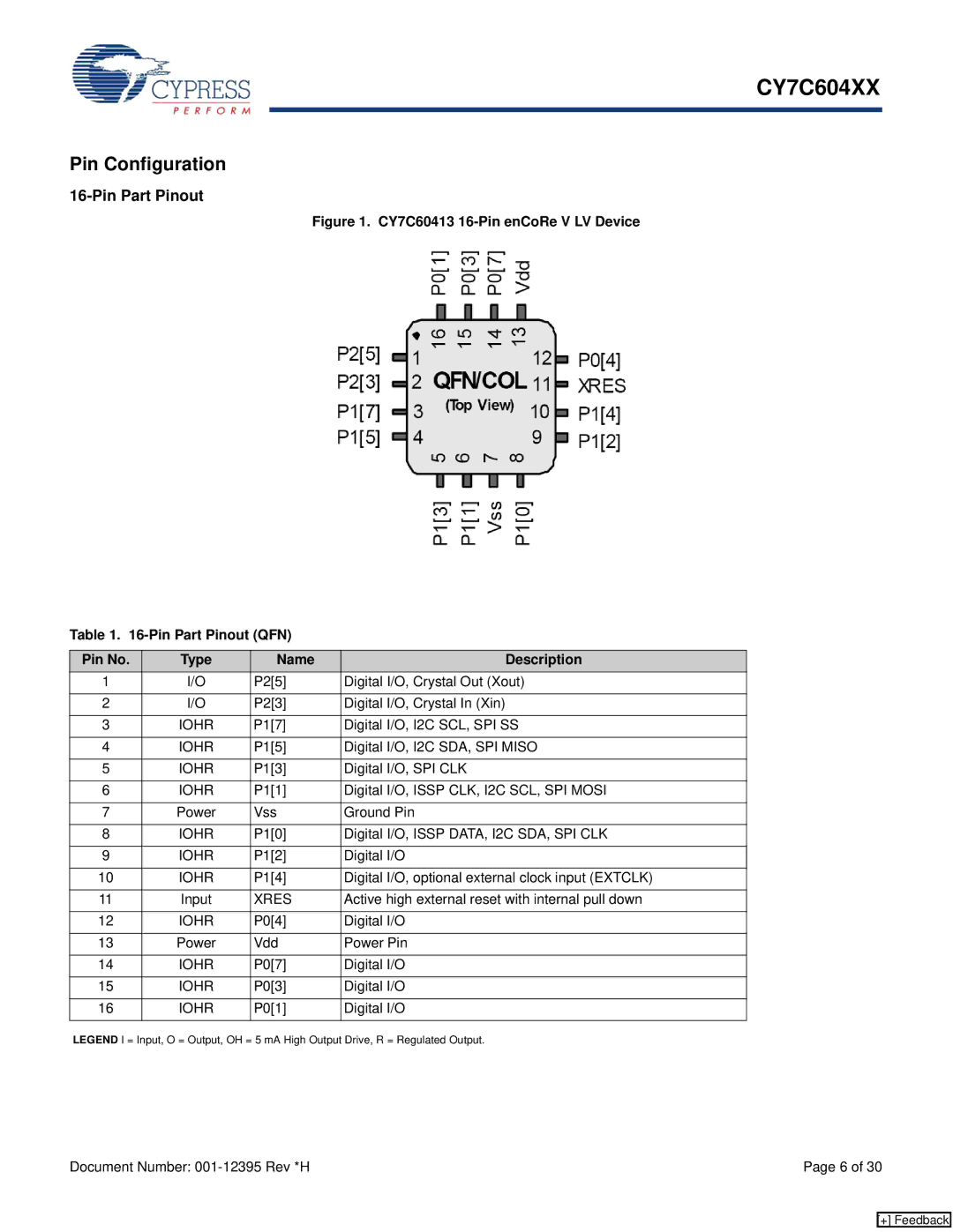
16-Pin Part Pinout
Figure 1. CY7C60413 16-Pin enCoRe V LV Device
Table 1. 16-Pin Part Pinout (QFN)
Pin No. | Type | Name | Description |
1 | I/O | P2[5] | Digital I/O, Crystal Out (Xout) |
|
|
|
|
2 | I/O | P2[3] | Digital I/O, Crystal In (Xin) |
|
|
|
|
3 | IOHR | P1[7] | Digital I/O, I2C SCL, SPI SS |
|
|
|
|
4 | IOHR | P1[5] | Digital I/O, I2C SDA, SPI MISO |
|
|
|
|
5 | IOHR | P1[3] | Digital I/O, SPI CLK |
|
|
|
|
6 | IOHR | P1[1] | Digital I/O, ISSP CLK, I2C SCL, SPI MOSI |
|
|
|
|
7 | Power | Vss | Ground Pin |
|
|
|
|
8 | IOHR | P1[0] | Digital I/O, ISSP DATA, I2C SDA, SPI CLK |
|
|
|
|
9 | IOHR | P1[2] | Digital I/O |
|
|
|
|
10 | IOHR | P1[4] | Digital I/O, optional external clock input (EXTCLK) |
|
|
|
|
11 | Input | XRES | Active high external reset with internal pull down |
|
|
|
|
12 | IOHR | P0[4] | Digital I/O |
|
|
|
|
13 | Power | Vdd | Power Pin |
|
|
|
|
14 | IOHR | P0[7] | Digital I/O |
|
|
|
|
15 | IOHR | P0[3] | Digital I/O |
|
|
|
|
16 | IOHR | P0[1] | Digital I/O |
|
|
|
|
LEGEND I = Input, O = Output, OH = 5 mA High Output Drive, R = Regulated Output.
Document Number: | Page 6 of 30 |
[+] Feedback