CY7C604XX
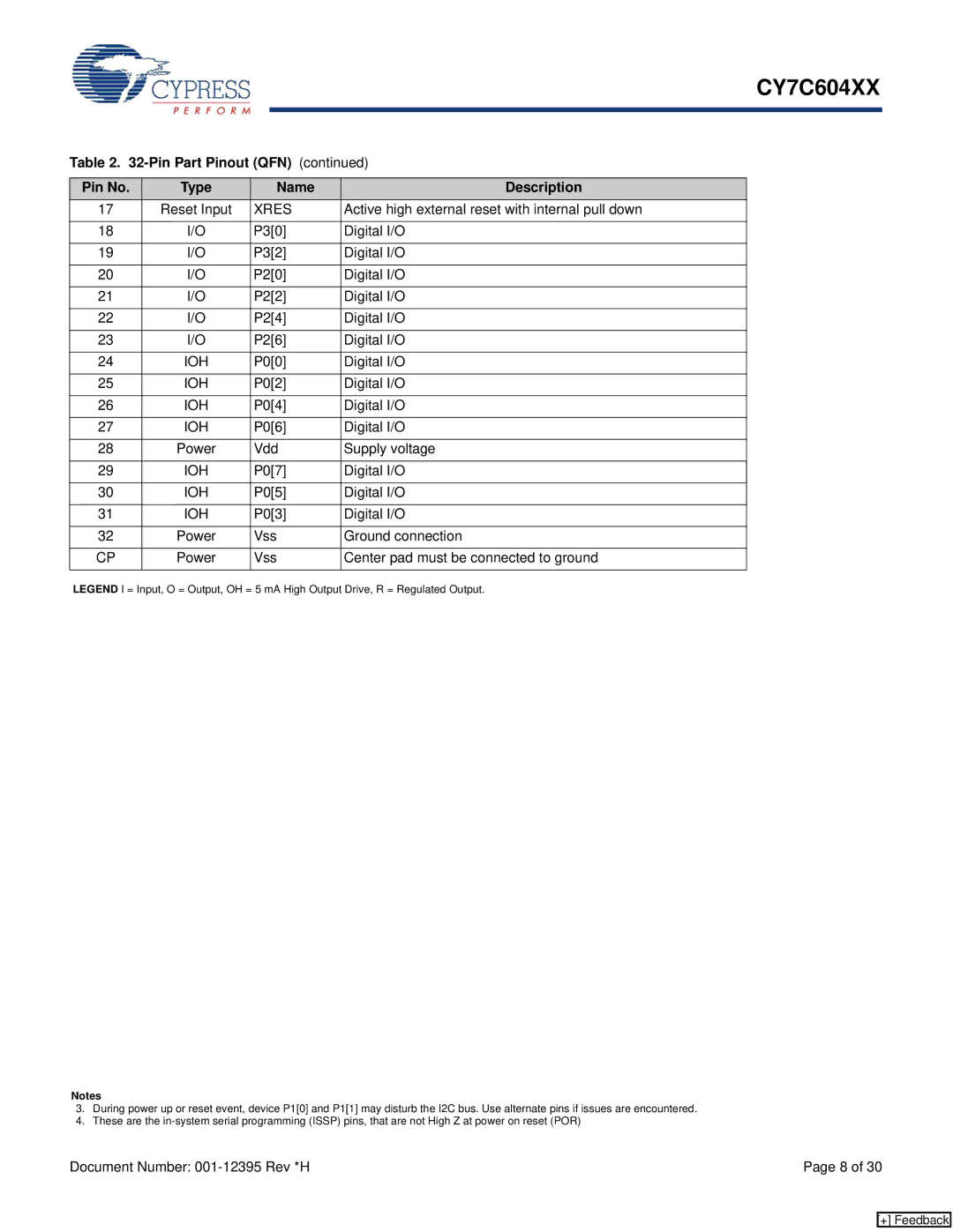
Table 2. 32-Pin Part Pinout (QFN) (continued)
Pin No. | Type | Name | Description |
17 | Reset Input | XRES | Active high external reset with internal pull down |
|
|
|
|
18 | I/O | P3[0] | Digital I/O |
|
|
|
|
19 | I/O | P3[2] | Digital I/O |
|
|
|
|
20 | I/O | P2[0] | Digital I/O |
|
|
|
|
21 | I/O | P2[2] | Digital I/O |
|
|
|
|
22 | I/O | P2[4] | Digital I/O |
|
|
|
|
23 | I/O | P2[6] | Digital I/O |
|
|
|
|
24 | IOH | P0[0] | Digital I/O |
|
|
|
|
25 | IOH | P0[2] | Digital I/O |
|
|
|
|
26 | IOH | P0[4] | Digital I/O |
|
|
|
|
27 | IOH | P0[6] | Digital I/O |
|
|
|
|
28 | Power | Vdd | Supply voltage |
|
|
|
|
29 | IOH | P0[7] | Digital I/O |
|
|
|
|
30 | IOH | P0[5] | Digital I/O |
|
|
|
|
31 | IOH | P0[3] | Digital I/O |
|
|
|
|
32 | Power | Vss | Ground connection |
|
|
|
|
CP | Power | Vss | Center pad must be connected to ground |
|
|
|
|
LEGEND I = Input, O = Output, OH = 5 mA High Output Drive, R = Regulated Output.
Notes
3.During power up or reset event, device P1[0] and P1[1] may disturb the I2C bus. Use alternate pins if issues are encountered.
4.These are the
Document Number: | Page 8 of 30 |
[+] Feedback