CY7C604XX
DC General Purpose I/O Specifications
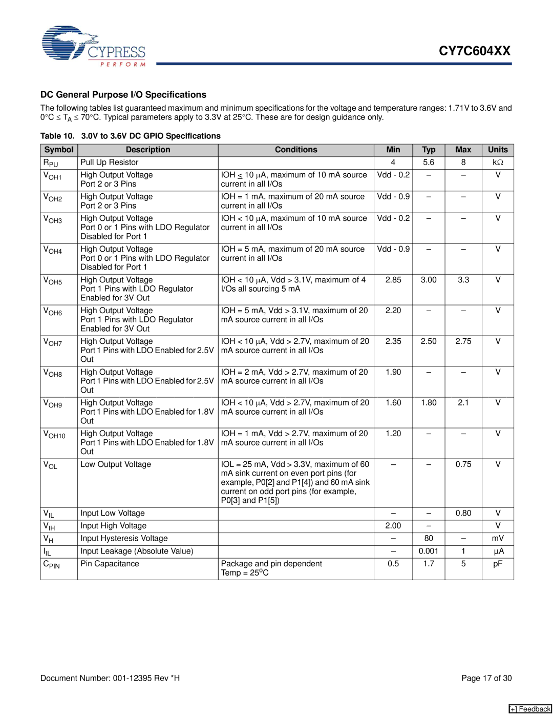
The following tables list guaranteed maximum and minimum specifications for the voltage and temperature ranges: 1.71V to 3.6V and 0°C ≤ TA ≤ 70°C. Typical parameters apply to 3.3V at 25°C. These are for design guidance only.
Table 10. 3.0V to 3.6V DC GPIO Specifications
Symbol | Description | Conditions | Min | Typ | Max | Units |
RPU | Pull Up Resistor |
| 4 | 5.6 | 8 | kΩ |
VOH1 | High Output Voltage | IOH < 10 μA, maximum of 10 mA source | Vdd - 0.2 | – | – | V |
| Port 2 or 3 Pins | current in all I/Os |
|
|
|
|
VOH2 | High Output Voltage | IOH = 1 mA, maximum of 20 mA source | Vdd - 0.9 | – | – | V |
| Port 2 or 3 Pins | current in all I/Os |
|
|
|
|
VOH3 | High Output Voltage | IOH < 10 μA, maximum of 10 mA source | Vdd - 0.2 | – | – | V |
| Port 0 or 1 Pins with LDO Regulator | current in all I/Os |
|
|
|
|
| Disabled for Port 1 |
|
|
|
|
|
VOH4 | High Output Voltage | IOH = 5 mA, maximum of 20 mA source | Vdd - 0.9 | – | – | V |
| Port 0 or 1 Pins with LDO Regulator | current in all I/Os |
|
|
|
|
| Disabled for Port 1 |
|
|
|
|
|
VOH5 | High Output Voltage | IOH < 10 μA, Vdd > 3.1V, maximum of 4 | 2.85 | 3.00 | 3.3 | V |
| Port 1 Pins with LDO Regulator | I/Os all sourcing 5 mA |
|
|
|
|
| Enabled for 3V Out |
|
|
|
|
|
VOH6 | High Output Voltage | IOH = 5 mA, Vdd > 3.1V, maximum of 20 | 2.20 | – | – | V |
| Port 1 Pins with LDO Regulator | mA source current in all I/Os |
|
|
|
|
| Enabled for 3V Out |
|
|
|
|
|
VOH7 | High Output Voltage | IOH < 10 μA, Vdd > 2.7V, maximum of 20 | 2.35 | 2.50 | 2.75 | V |
| Port 1 Pins with LDO Enabled for 2.5V | mA source current in all I/Os |
|
|
|
|
| Out |
|
|
|
|
|
VOH8 | High Output Voltage | IOH = 2 mA, Vdd > 2.7V, maximum of 20 | 1.90 | – | – | V |
| Port 1 Pins with LDO Enabled for 2.5V | mA source current in all I/Os |
|
|
|
|
| Out |
|
|
|
|
|
VOH9 | High Output Voltage | IOH < 10 μA, Vdd > 2.7V, maximum of 20 | 1.60 | 1.80 | 2.1 | V |
| Port 1 Pins with LDO Enabled for 1.8V | mA source current in all I/Os |
|
|
|
|
| Out |
|
|
|
|
|
VOH10 | High Output Voltage | IOH = 1 mA, Vdd > 2.7V, maximum of 20 | 1.20 | – | – | V |
| Port 1 Pins with LDO Enabled for 1.8V | mA source current in all I/Os |
|
|
|
|
| Out |
|
|
|
|
|
VOL | Low Output Voltage | IOL = 25 mA, Vdd > 3.3V, maximum of 60 | – | – | 0.75 | V |
|
| mA sink current on even port pins (for |
|
|
|
|
|
| example, P0[2] and P1[4]) and 60 mA sink |
|
|
|
|
|
| current on odd port pins (for example, |
|
|
|
|
|
| P0[3] and P1[5]) |
|
|
|
|
VIL | Input Low Voltage |
| – | – | 0.80 | V |
VIH | Input High Voltage |
| 2.00 | – |
| V |
VH | Input Hysteresis Voltage |
| – | 80 | – | mV |
IIL | Input Leakage (Absolute Value) |
| – | 0.001 | 1 | µA |
CPIN | Pin Capacitance | Package and pin dependent | 0.5 | 1.7 | 5 | pF |
|
| Temp = 25oC |
|
|
|
|
Document Number: | Page 17 of 30 |
[+] Feedback