CY7C604XX
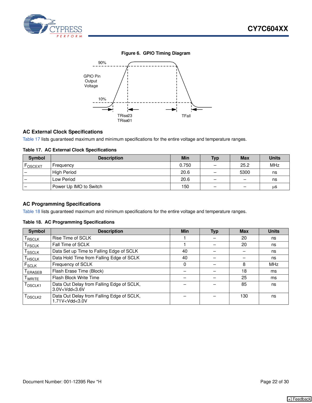
Figure 6. GPIO Timing Diagram
90%
GPIO Pin
Output
Voltage
10%
TRise23 | TFall |
TRise01 |
|
AC External Clock Specifications
Table 17 lists guaranteed maximum and minimum specifications for the entire voltage and temperature ranges.
Table 17. AC External Clock Specifications
Symbol | Description | Min | Typ | Max | Units |
FOSCEXT | Frequency | 0.750 | – | 25.2 | MHz |
– | High Period | 20.6 | – | 5300 | ns |
– | Low Period | 20.6 | – | – | ns |
– | Power Up IMO to Switch | 150 | – | – | μs |
AC Programming Specifications
Table 18 lists guaranteed maximum and minimum specifications for the entire voltage and temperature ranges.
Table 18. AC Programming Specifications
Symbol | Description | Min | Typ | Max | Units |
TRSCLK | Rise Time of SCLK | 1 | – | 20 | ns |
TFSCLK | Fall Time of SCLK | 1 | – | 20 | ns |
TSSCLK | Data Set up Time to Falling Edge of SCLK | 40 | – | – | ns |
THSCLK | Data Hold Time from Falling Edge of SCLK | 40 | – | – | ns |
FSCLK | Frequency of SCLK | 0 | – | 8 | MHz |
TERASEB | Flash Erase Time (Block) | – | – | 18 | ms |
TWRITE | Flash Block Write Time | – | – | 25 | ms |
TDSCLK1 | Data Out Delay from Falling Edge of SCLK, | – | – | 85 | ns |
| 3.0V<Vdd<3.6V |
|
|
|
|
TDSCLK2 | Data Out Delay from Falling Edge of SCLK, | – | – | 130 | ns |
| 1.71V<Vdd<3.0V |
|
|
|
|
Document Number: | Page 22 of 30 |
[+] Feedback