CY7C604XX
32-Pin Part Pinout
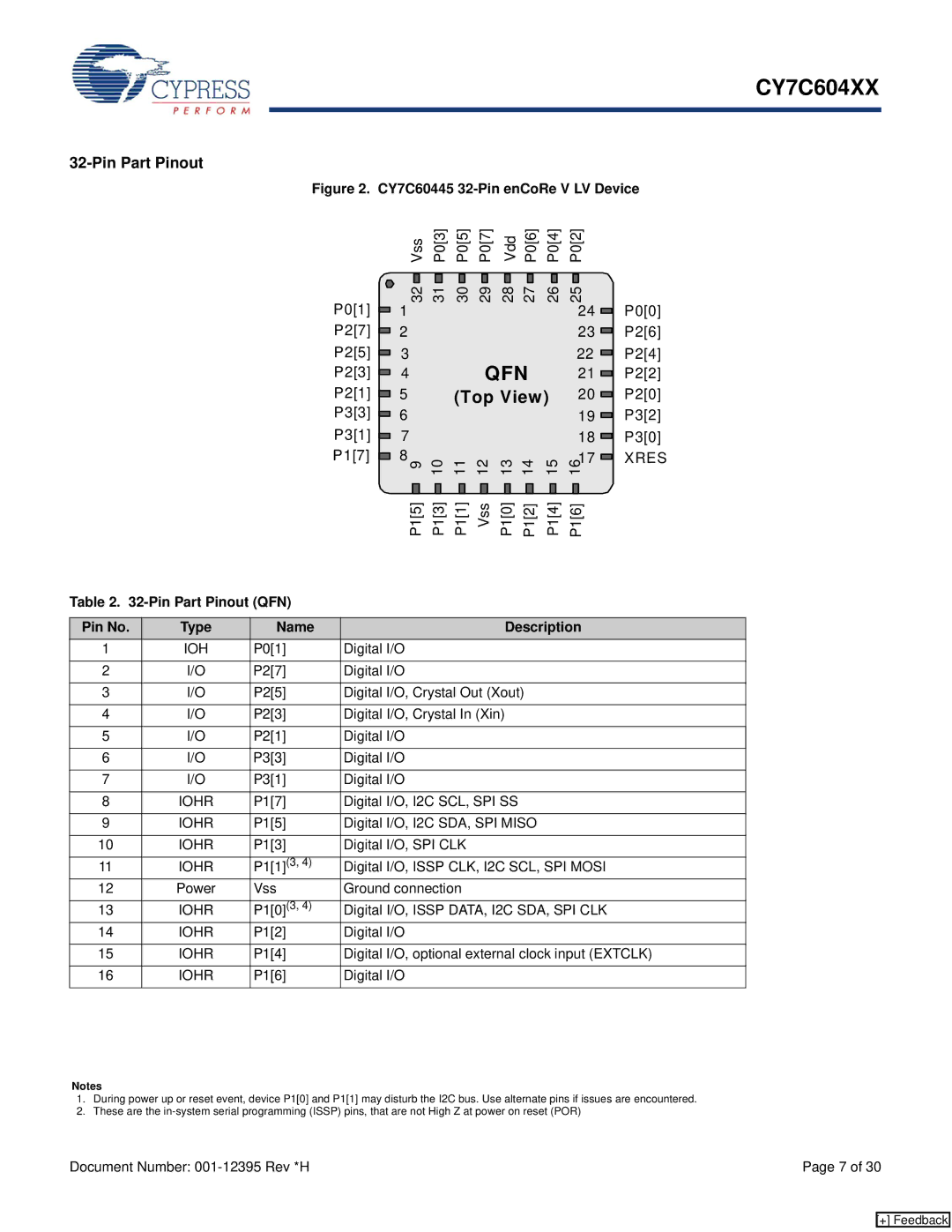
Figure 2. CY7C60445 32-Pin enCoRe V LV Device
P0[1] ![]() P2[7]
P2[7] ![]() P2[5]
P2[5] ![]() P2[3]
P2[3] ![]() P2[1]
P2[1] ![]() P3[3]
P3[3] ![]() P3[1]
P3[1] ![]() P1[7]
P1[7] ![]()
Vss
32 1
2
3
4
5
6
7
8 9
P1[5]
P0[3] | P0[5] | P0[7] | Vdd | P0[6] | P0[4] | |||||||||||
|
|
|
|
|
|
|
|
|
|
|
|
|
|
| ||
|
|
|
|
|
|
|
|
|
|
|
|
|
|
|
|
|
31 | 30 | 29 | 28 | 27 | 26 | |||||||||||
QFN
(Top View)
10 | 11 |
| 12 |
| 13 | 14 |
| 15 | |||||||||
|
|
|
|
|
|
|
|
|
|
|
|
|
|
|
| ||
|
|
|
|
|
|
|
|
|
|
|
|
|
|
|
|
|
|
P1[3] | P1[1] | Vss | P1[0] | P1[2] | P1[4] | ||||||||||||
P0[2]
25 24 ![]()
23 ![]()
22![]()
21 ![]()
20 ![]()
19 ![]()
18 ![]()
17 ![]() 16
16
P1[6]
P0[0]
P2[6]
P2[4]
P2[2]
P2[0]
P3[2]
P3[0]
XRES
Table 2. 32-Pin Part Pinout (QFN)
Pin No. | Type | Name | Description |
1 | IOH | P0[1] | Digital I/O |
|
|
|
|
2 | I/O | P2[7] | Digital I/O |
|
|
|
|
3 | I/O | P2[5] | Digital I/O, Crystal Out (Xout) |
|
|
|
|
4 | I/O | P2[3] | Digital I/O, Crystal In (Xin) |
|
|
|
|
5 | I/O | P2[1] | Digital I/O |
|
|
|
|
6 | I/O | P3[3] | Digital I/O |
|
|
|
|
7 | I/O | P3[1] | Digital I/O |
|
|
|
|
8 | IOHR | P1[7] | Digital I/O, I2C SCL, SPI SS |
|
|
|
|
9 | IOHR | P1[5] | Digital I/O, I2C SDA, SPI MISO |
|
|
|
|
10 | IOHR | P1[3] | Digital I/O, SPI CLK |
|
|
|
|
11 | IOHR | P1[1](3, 4) | Digital I/O, ISSP CLK, I2C SCL, SPI MOSI |
12 | Power | Vss | Ground connection |
|
|
|
|
13 | IOHR | P1[0](3, 4) | Digital I/O, ISSP DATA, I2C SDA, SPI CLK |
14 | IOHR | P1[2] | Digital I/O |
|
|
|
|
15 | IOHR | P1[4] | Digital I/O, optional external clock input (EXTCLK) |
|
|
|
|
16 | IOHR | P1[6] | Digital I/O |
|
|
|
|
Notes
1.During power up or reset event, device P1[0] and P1[1] may disturb the I2C bus. Use alternate pins if issues are encountered.
2.These are the
Document Number: | Page 7 of 30 |
[+] Feedback