CY7C604XX
Package Diagram
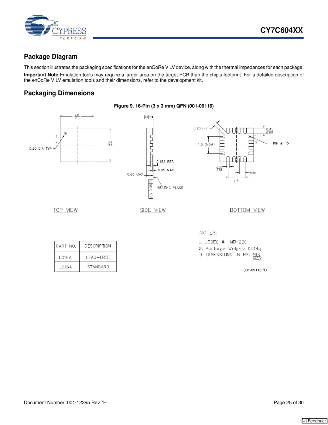
This section illustrates the packaging specifications for the enCoRe V LV device, along with the thermal impedances for each package.
Important Note Emulation tools may require a larger area on the target PCB than the chip’s footprint. For a detailed description of the enCoRe V LV emulation tools and their dimensions, refer to the development kit.
Packaging Dimensions
Figure 9. 16-Pin (3 x 3 mm) QFN (001-09116)
Document Number: | Page 25 of 30 |
[+] Feedback