CY8C23433, CY8C23533
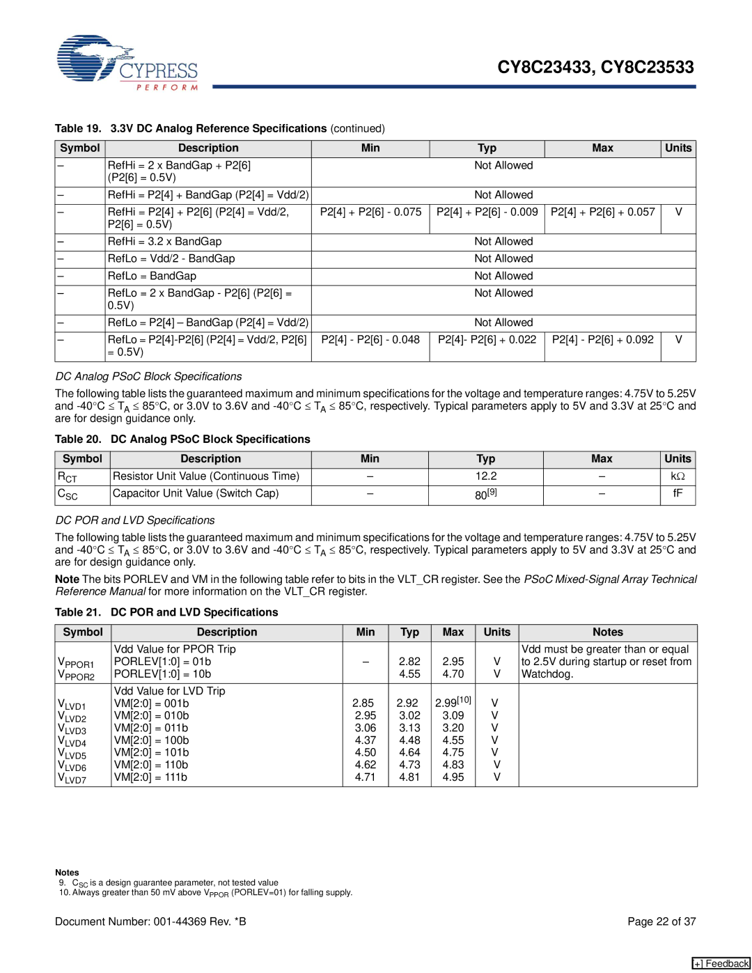
Table 19. 3.3V DC Analog Reference Specifications (continued)
Symbol | Description | Min | Typ | Max | Units |
– | RefHi = 2 x BandGap + P2[6] |
| Not Allowed |
|
|
| (P2[6] = 0.5V) |
|
|
|
|
– | RefHi = P2[4] + BandGap (P2[4] = Vdd/2) |
| Not Allowed |
|
|
|
|
|
|
|
|
– | RefHi = P2[4] + P2[6] (P2[4] = Vdd/2, | P2[4] + P2[6] - 0.075 | P2[4] + P2[6] - 0.009 | P2[4] + P2[6] + 0.057 | V |
| P2[6] = 0.5V) |
|
|
|
|
– | RefHi = 3.2 x BandGap |
| Not Allowed |
|
|
|
|
|
|
|
|
– | RefLo = Vdd/2 - BandGap |
| Not Allowed |
|
|
|
|
|
|
|
|
– | RefLo = BandGap |
| Not Allowed |
|
|
|
|
|
|
|
|
– | RefLo = 2 x BandGap - P2[6] (P2[6] = |
| Not Allowed |
|
|
| 0.5V) |
|
|
|
|
– | RefLo = P2[4] – BandGap (P2[4] = Vdd/2) |
| Not Allowed |
|
|
|
|
|
|
|
|
– | RefLo = | P2[4] - P2[6] - 0.048 | P2[4]- P2[6] + 0.022 | P2[4] - P2[6] + 0.092 | V |
| = 0.5V) |
|
|
|
|
DC Analog PSoC Block Specifications
The following table lists the guaranteed maximum and minimum specifications for the voltage and temperature ranges: 4.75V to 5.25V and
Table 20. DC Analog PSoC Block Specifications
Symbol | Description | Min | Typ | Max | Units |
RCT | Resistor Unit Value (Continuous Time) | – | 12.2 | – | kΩ |
CSC | Capacitor Unit Value (Switch Cap) | – | 80[9] | – | fF |
DC POR and LVD Specifications
The following table lists the guaranteed maximum and minimum specifications for the voltage and temperature ranges: 4.75V to 5.25V and
Note The bits PORLEV and VM in the following table refer to bits in the VLT_CR register. See the PSoC
Table 21. DC POR and LVD Specifications
Symbol | Description | Min | Typ | Max | Units | Notes |
VPPOR1 | Vdd Value for PPOR Trip |
|
|
|
| Vdd must be greater than or equal |
PORLEV[1:0] = 01b | – | 2.82 | 2.95 | V | to 2.5V during startup or reset from | |
VPPOR2 | PORLEV[1:0] = 10b |
| 4.55 | 4.70 | V | Watchdog. |
| Vdd Value for LVD Trip | 2.85 | 2.92 | 2.99[10] | V |
|
VLVD1 | VM[2:0] = 001b |
| ||||
VLVD2 | VM[2:0] = 010b | 2.95 | 3.02 | 3.09 | V |
|
VLVD3 | VM[2:0] = 011b | 3.06 | 3.13 | 3.20 | V |
|
VLVD4 | VM[2:0] = 100b | 4.37 | 4.48 | 4.55 | V |
|
VLVD5 | VM[2:0] = 101b | 4.50 | 4.64 | 4.75 | V |
|
VLVD6 | VM[2:0] = 110b | 4.62 | 4.73 | 4.83 | V |
|
VLVD7 | VM[2:0] = 111b | 4.71 | 4.81 | 4.95 | V |
|
Notes
9.CSC is a design guarantee parameter, not tested value
10.Always greater than 50 mV above VPPOR (PORLEV=01) for falling supply.
Document Number: | Page 22 of 37 |
[+] Feedback