CY8C23433, CY8C23533
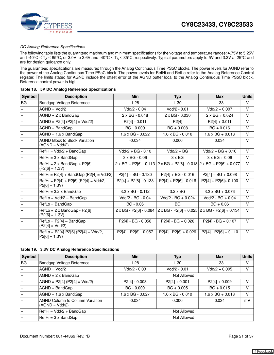
DC Analog Reference Specifications
The following table lists the guaranteed maximum and minimum specifications for the voltage and temperature ranges: 4.75V to 5.25V and
The guaranteed specifications are measured through the Analog Continuous Time PSoC blocks. The power levels for AGND refer to the power of the Analog Continuous Time PSoC block. The power levels for RefHi and RefLo refer to the Analog Reference Control register. The limits stated for AGND include the offset error of the AGND buffer local to the Analog Continuous Time PSoC block. Reference control power is high.
Table 18. 5V DC Analog Reference Specifications
Symbol | Description | Min | Typ | Max | Units |
|
BG | Bandgap Voltage Reference | 1.28 | 1.30 | 1.33 | V |
|
|
|
|
|
|
|
|
– | AGND = Vdd/2 | Vdd/2 - 0.04 | Vdd/2 - 0.01 | Vdd/2 + 0.007 | V |
|
|
|
|
|
|
|
|
– | AGND = 2 x BandGap | 2 x BG - 0.048 | 2 x BG - 0.030 | 2 x BG + 0.024 | V |
|
|
|
|
|
|
|
|
– | AGND = P2[4] (P2[4] = Vdd/2) | P2[4] - 0.011 | P2[4] | P2[4] + 0.011 | V |
|
|
|
|
|
|
|
|
– | AGND = BandGap | BG - 0.009 | BG + 0.008 | BG + 0.016 | V |
|
|
|
|
|
|
|
|
– | AGND = 1.6 x BandGap | 1.6 x BG - 0.022 | 1.6 x BG - 0.010 | 1.6 x BG + 0.018 | V |
|
|
|
|
|
|
|
|
– | AGND Block to Block Variation | 0.000 | 0.034 | V |
| |
| (AGND = Vdd/2) |
|
|
|
|
|
– | RefHi = Vdd/2 + BandGap | Vdd/2 + BG - 0.10 | Vdd/2 + BG | Vdd/2 + BG + 0.10 | V |
|
|
|
|
|
|
|
|
– | RefHi = 3 x BandGap | 3 x BG - 0.06 | 3 x BG | 3 x BG + 0.06 | V |
|
|
|
|
|
|
|
|
– | RefHi = 2 x BandGap + P2[6] | 2 x BG + P2[6] - 0.113 | 2 x BG + P2[6] - 0.018 | 2 x BG + P2[6] + 0.077 | V |
|
| (P2[6] = 1.3V) |
|
|
|
|
|
– | RefHi = P2[4] + BandGap (P2[4] = Vdd/2) | P2[4] + BG - 0.130 | P2[4] + BG - 0.016 | P2[4] + BG + 0.098 | V |
|
|
|
|
|
|
|
|
– | RefHi = P2[4] + P2[6] (P2[4] = Vdd/2, | P2[4] + P2[6] - 0.133 | P2[4] + P2[6] - 0.016 | P2[4] + P2[6]+ 0.100 | V |
|
| P2[6] = 1.3V) |
|
|
|
|
|
– | RefHi = 3.2 x BandGap | 3.2 x BG - 0.112 | 3.2 x BG | 3.2 x BG + 0.076 | V |
|
|
|
|
|
|
|
|
– | RefLo = Vdd/2 – BandGap | Vdd/2 - BG - 0.04 | Vdd/2 - BG + 0.024 | Vdd/2 - BG + 0.04 | V |
|
|
|
|
|
|
|
|
– | RefLo = BandGap | BG - 0.06 | BG | BG + 0.06 | V |
|
|
|
|
|
|
|
|
– | RefLo = 2 x BandGap - P2[6] | 2 x BG - P2[6] - 0.084 | 2 x BG - P2[6] + 0.025 | 2 x BG - P2[6] + 0.134 | V |
|
| (P2[6] = 1.3V) |
|
|
|
|
|
– | RefLo = P2[4] – BandGap | P2[4] - BG - 0.056 | P2[4] - BG + 0.026 | P2[4] - BG + 0.107 | V |
|
| (P2[4] = Vdd/2) |
|
|
|
|
|
– | RefLo = | P2[4] - P2[6] - 0.057 | P2[4] - P2[6] + 0.026 | P2[4] - P2[6] + 0.110 | V |
|
| P2[6] = 1.3V) |
|
|
|
|
|
Table 19. 3.3V DC Analog Reference Specifications |
|
|
|
| ||
|
|
|
|
|
|
|
Symbol | Description | Min | Typ | Max | Units |
|
BG | Bandgap Voltage Reference | 1.28 | 1.30 | 1.33 | V |
|
– | AGND = Vdd/2 | Vdd/2 - 0.03 | Vdd/2 - 0.01 | Vdd/2 + 0.005 | V |
|
|
|
|
|
|
|
|
– | AGND = 2 x BandGap |
| Not Allowed |
|
|
|
– | AGND = P2[4] (P2[4] = Vdd/2) | P2[4] - 0.008 | P2[4] + 0.001 | P2[4] + 0.009 | V |
|
– | AGND = BandGap | BG - 0.009 | BG + 0.005 | BG + 0.015 | V |
|
– | AGND = 1.6 x BandGap | 1.6 x BG - 0.027 | 1.6 x BG - 0.010 | 1.6 x BG + 0.018 | V |
|
– | AGND Column to Column Variation | 0.000 | 0.034 | mV |
| |
| (AGND = Vdd/2) |
|
|
|
|
|
– | RefHi = Vdd/2 + BandGap |
| Not Allowed |
|
|
|
|
|
|
|
|
|
|
– | RefHi = 3 x BandGap |
| Not Allowed |
|
|
|
Document Number: |
|
| Page 21 of 37 |
| ||
[+] Feedback