CY8C23433, CY8C23533
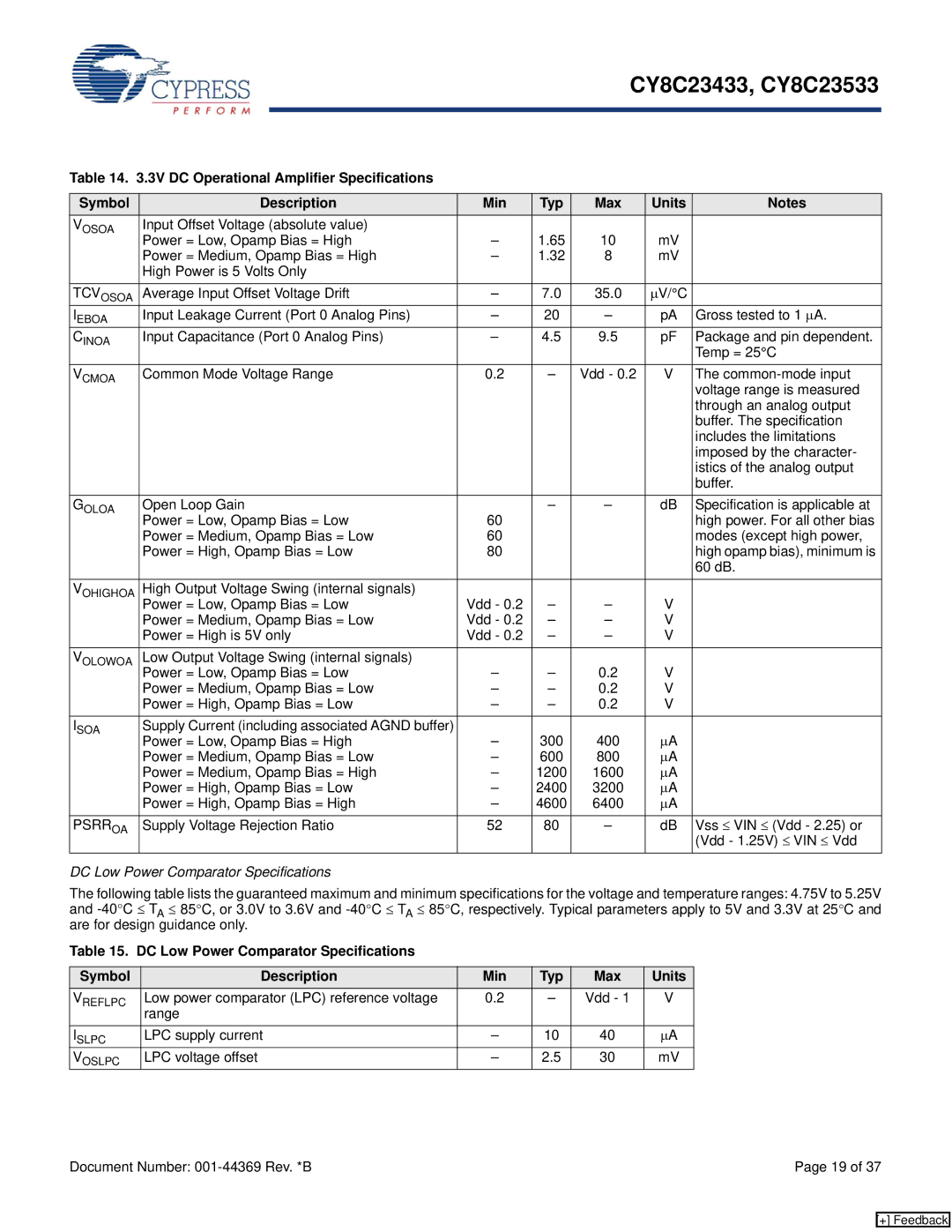
Table 14. 3.3V DC Operational Amplifier Specifications
Symbol | Description | Min | Typ | Max | Units | Notes |
VOSOA | Input Offset Voltage (absolute value) | – | 1.65 | 10 | mV |
|
| Power = Low, Opamp Bias = High |
| ||||
| Power = Medium, Opamp Bias = High | – | 1.32 | 8 | mV |
|
| High Power is 5 Volts Only |
|
|
|
|
|
TCVOSOA | Average Input Offset Voltage Drift | – | 7.0 | 35.0 | μV/°C |
|
IEBOA | Input Leakage Current (Port 0 Analog Pins) | – | 20 | – | pA | Gross tested to 1 μA. |
CINOA | Input Capacitance (Port 0 Analog Pins) | – | 4.5 | 9.5 | pF | Package and pin dependent. |
|
|
|
|
|
| Temp = 25°C |
VCMOA | Common Mode Voltage Range | 0.2 | – | Vdd - 0.2 | V | The |
|
|
|
|
|
| voltage range is measured |
|
|
|
|
|
| through an analog output |
|
|
|
|
|
| buffer. The specification |
|
|
|
|
|
| includes the limitations |
|
|
|
|
|
| imposed by the character- |
|
|
|
|
|
| istics of the analog output |
|
|
|
|
|
| buffer. |
GOLOA | Open Loop Gain | 60 | – | – | dB | Specification is applicable at |
| Power = Low, Opamp Bias = Low |
|
|
| high power. For all other bias | |
| Power = Medium, Opamp Bias = Low | 60 |
|
|
| modes (except high power, |
| Power = High, Opamp Bias = Low | 80 |
|
|
| high opamp bias), minimum is |
|
|
|
|
|
| 60 dB. |
VOHIGHOA | High Output Voltage Swing (internal signals) | Vdd - 0.2 | – | – | V |
|
| Power = Low, Opamp Bias = Low |
| ||||
| Power = Medium, Opamp Bias = Low | Vdd - 0.2 | – | – | V |
|
| Power = High is 5V only | Vdd - 0.2 | – | – | V |
|
VOLOWOA | Low Output Voltage Swing (internal signals) | – | – | 0.2 | V |
|
| Power = Low, Opamp Bias = Low |
| ||||
| Power = Medium, Opamp Bias = Low | – | – | 0.2 | V |
|
| Power = High, Opamp Bias = Low | – | – | 0.2 | V |
|
ISOA | Supply Current (including associated AGND buffer) | – | 300 | 400 | μA |
|
| Power = Low, Opamp Bias = High |
| ||||
| Power = Medium, Opamp Bias = Low | – | 600 | 800 | μA |
|
| Power = Medium, Opamp Bias = High | – | 1200 | 1600 | μA |
|
| Power = High, Opamp Bias = Low | – | 2400 | 3200 | μA |
|
| Power = High, Opamp Bias = High | – | 4600 | 6400 | μA |
|
PSRROA | Supply Voltage Rejection Ratio | 52 | 80 | – | dB | Vss ≤ VIN ≤ (Vdd - 2.25) or |
|
|
|
|
|
| (Vdd - 1.25V) ≤ VIN ≤ Vdd |
DC Low Power Comparator Specifications
The following table lists the guaranteed maximum and minimum specifications for the voltage and temperature ranges: 4.75V to 5.25V and
Table 15. DC Low Power Comparator Specifications
Symbol | Description | Min | Typ | Max | Units |
VREFLPC | Low power comparator (LPC) reference voltage | 0.2 | – | Vdd - 1 | V |
| range |
|
|
|
|
ISLPC | LPC supply current | – | 10 | 40 | μA |
VOSLPC | LPC voltage offset | – | 2.5 | 30 | mV |
Document Number: | Page 19 of 37 |
[+] Feedback
