CY8C23433, CY8C23533
PSoC Functional Overview
The PSoC family consists of many
The PSoC architecture, as shown in the Logic Block Diagram on page 1, consists of four main areas: PSoC Core, Digital System, Analog System, and System Resources. Configurable global busing allows combining all the device resources into a complete custom system. The PSoC CY8C23x33 family can have up to three IO ports that connect to the global digital and analog interconnects, providing access to four digital blocks and four analog blocks.
PSoC Core
The PSoC Core is a powerful engine that supports a rich feature set. The core includes a CPU, memory, clocks, and configurable GPIO (General Purpose IO).
The M8C CPU core is a powerful processor with speeds up to 24 MHz, providing a four MIPS
Memory encompasses 8 KB of Flash for program storage, 256 bytes of SRAM for data storage, and up to 2 KB of EEPROM emulated using the Flash. Program Flash uses four protection levels on blocks of 64 bytes, allowing customized software IP protection.
The PSoC device incorporates flexible internal clock generators, including a 24 MHz IMO (internal main oscillator) accurate to ±2.5% over temperature and voltage. The 24 MHz IMO can also be doubled to 48 MHz for use by the digital system. A low power 32 kHz ILO (internal low speed oscillator) is provided for the Sleep timer and WDT. If crystal accuracy is desired, the ECO (32.768 kHz external crystal oscillator) is available for use as a Real Time Clock (RTC) and can optionally generate a
PSoC GPIOs provide connection to the CPU, digital and analog resources of the device. Each pin’s drive mode may be selected from eight options, allowing great flexibility in external interfacing. Every pin also has the capability to generate a system interrupt on high level, low level, and change from last read.
Document Number:
Digital System
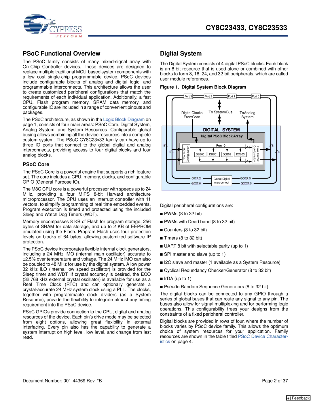
The Digital System consists of 4 digital PSoC blocks. Each block is an
Figure 1. Digital System Block Diagram
Port 3 |
| Port 2 |
| Port 1 |
| Port 0 |
DigitalClocks | To SystemBus | ToAnalog | |
FromCore |
|
| System |
|
| ||
|
|
|
|
|
| DIGITAL SYSTEM |
|
| |||
|
| Digital PSoC Block Array |
|
| |||
8 | Configuration |
| Row 0 | 4 | Row Output Configuration | 8 | |
8 | DBB00 | DBB01 | DCB02 | DCB03 | 8 | ||
RowInput |
| ||||||
|
|
| 4 |
| |||
|
| GIE[7:0] | Global Digital | GOE[7:0] |
|
| |
|
| GIO[7:0] | Interconnect | GOO[7:0] |
|
| |
|
|
|
|
|
| ||
Digital peripheral configurations are:
■PWMs (8 to 32 bit)
■PWMs with Dead band (8 to 32 bit)
■Counters (8 to 32 bit)
■Timers (8 to 32 bit)
■UART 8 bit with selectable parity (up to 1)
■SPI master and slave (up to 1)
■I2C slave and master (1 available as a System Resource)
■Cyclical Redundancy Checker/Generator (8 to 32 bit)
■IrDA (up to 1)
■Pseudo Random Sequence Generators (8 to 32 bit)
The digital blocks can be connected to any GPIO through a series of global buses that can route any signal to any pin. The buses also allow for signal multiplexing and for performing logic operations. This configurability frees your designs from the constraints of a fixed peripheral controller.
Digital blocks are provided in rows of four, where the number of blocks varies by PSoC device family. This allows the optimum choice of system resources for your application. Family resources are shown in the table titled PSoC Device Character- istics on page 4.
Page 2 of 37
[+] Feedback