Interface
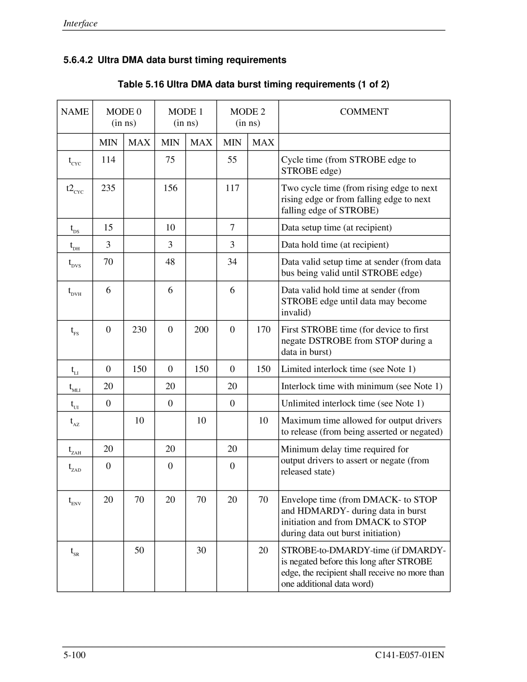
5.6.4.2 Ultra DMA data burst timing requirements
Table 5.16 Ultra DMA data burst timing requirements (1 of 2)
NAME | MODE 0 | MODE 1 | MODE 2 | COMMENT | |||
| (in ns) | (in ns) | (in ns) |
| |||
|
|
|
|
|
|
|
|
| MIN | MAX | MIN | MAX | MIN | MAX |
|
|
|
|
|
|
|
|
|
tCYC | 114 |
| 75 |
| 55 |
| Cycle time (from STROBE edge to |
|
|
|
|
|
|
| STROBE edge) |
|
|
|
|
|
|
|
|
t2CYC | 235 |
| 156 |
| 117 |
| Two cycle time (from rising edge to next |
|
|
|
|
|
|
| rising edge or from falling edge to next |
|
|
|
|
|
|
| falling edge of STROBE) |
|
|
|
|
|
|
|
|
tDS | 15 |
| 10 |
| 7 |
| Data setup time (at recipient) |
tDH | 3 |
| 3 |
| 3 |
| Data hold time (at recipient) |
tDVS | 70 |
| 48 |
| 34 |
| Data valid setup time at sender (from data |
|
|
|
|
|
|
| bus being valid until STROBE edge) |
|
|
|
|
|
|
|
|
tDVH | 6 |
| 6 |
| 6 |
| Data valid hold time at sender (from |
|
|
|
|
|
|
| STROBE edge until data may become |
|
|
|
|
|
|
| invalid) |
|
|
|
|
|
|
|
|
tFS | 0 | 230 | 0 | 200 | 0 | 170 | First STROBE time (for device to first |
|
|
|
|
|
|
| negate DSTROBE from STOP during a |
|
|
|
|
|
|
| data in burst) |
|
|
|
|
|
|
|
|
tLI | 0 | 150 | 0 | 150 | 0 | 150 | Limited interlock time (see Note 1) |
tMLI | 20 |
| 20 |
| 20 |
| Interlock time with minimum (see Note 1) |
tUI | 0 |
| 0 |
| 0 |
| Unlimited interlock time (see Note 1) |
tAZ |
| 10 |
| 10 |
| 10 | Maximum time allowed for output drivers |
|
|
|
|
|
|
| to release (from being asserted or negated) |
|
|
|
|
|
|
|
|
tZAH | 20 |
| 20 |
| 20 |
| Minimum delay time required for |
|
|
|
|
|
|
| output drivers to assert or negate (from |
tZAD | 0 |
| 0 |
| 0 |
| |
|
|
| released state) | ||||
|
|
|
|
|
|
| |
|
|
|
|
|
|
|
|
tENV | 20 | 70 | 20 | 70 | 20 | 70 | Envelope time (from DMACK- to STOP |
|
|
|
|
|
|
| and HDMARDY- during data in burst |
|
|
|
|
|
|
| initiation and from DMACK to STOP |
|
|
|
|
|
|
| during data out burst initiation) |
|
|
|
|
|
|
|
|
tSR |
| 50 |
| 30 |
| 20 | |
|
|
|
|
|
|
| is negated before this long after STROBE |
|
|
|
|
|
|
| edge, the recipient shall receive no more than |
|
|
|
|
|
|
| one additional data word) |
|
|
|
|
|
|
|
|