Contents
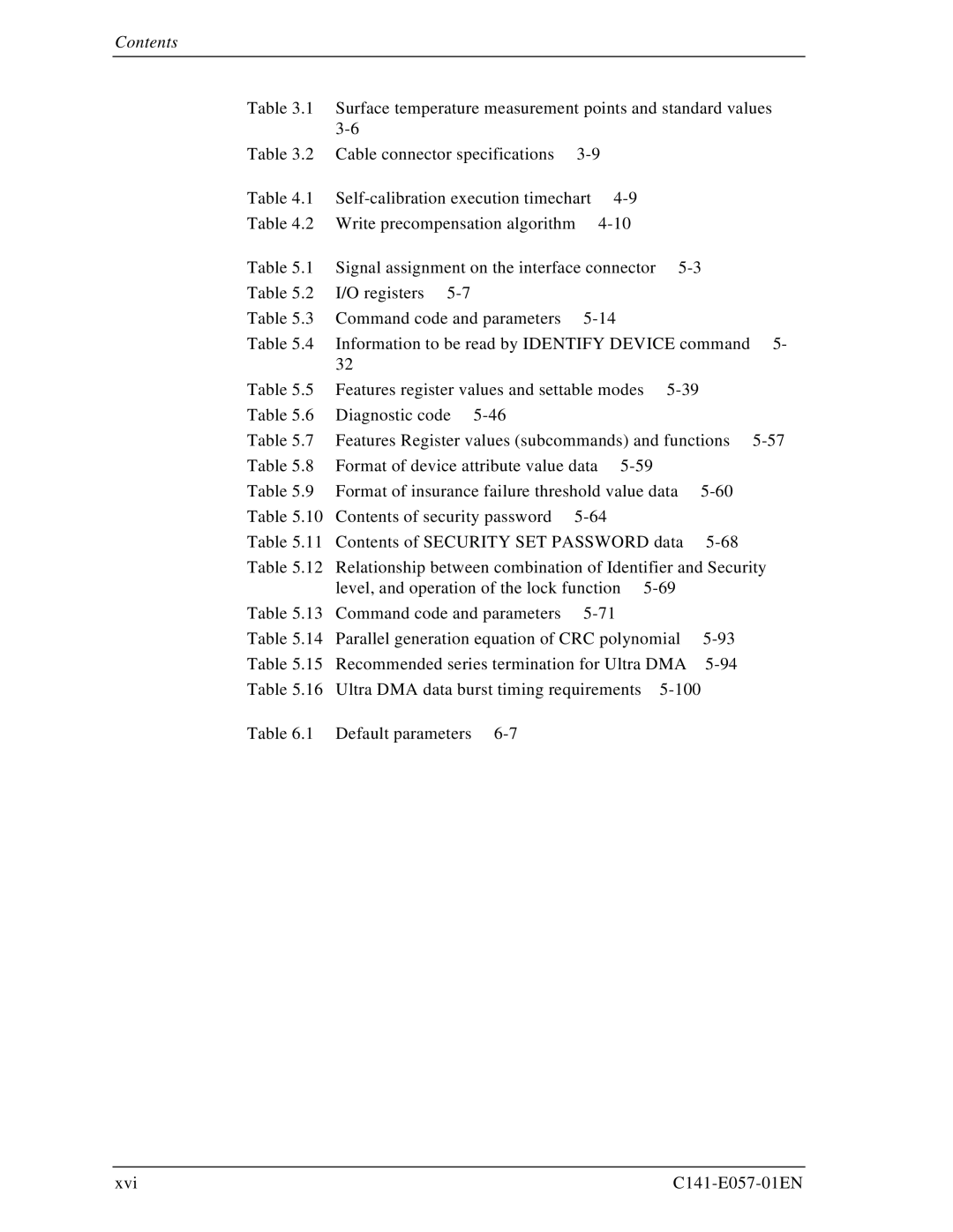
Table 3.1 | Surface temperature measurement points and standard values | ||||||
|
|
|
|
|
|
| |
Table 3.2 | Cable connector specifications |
|
|
| |||
Table 4.1 |
|
|
| ||||
Table 4.2 | Write precompensation algorithm |
|
|
| |||
Table 5.1 | Signal assignment on the interface connector |
| |||||
Table 5.2 | I/O registers |
|
|
|
|
|
|
Table 5.3 | Command code and parameters |
|
|
| |||
Table 5.4 | Information to be read by IDENTIFY DEVICE command | 5- | |||||
| 32 |
|
|
|
|
|
|
Table 5.5 | Features register values and settable modes |
|
| ||||
Table 5.6 | Diagnostic code |
|
|
|
|
| |
Table 5.7 | Features Register values (subcommands) and functions | ||||||
Table 5.8 | Format of device attribute value data |
|
|
| |||
Table 5.9 | Format of insurance failure threshold value data |
| |||||
Table 5.10 | Contents of security password |
|
|
| |||
Table 5.11 | Contents of SECURITY SET PASSWORD data |
| |||||
Table 5.12 | Relationship between combination of Identifier and Security | ||||||
| level, and operation of the lock function |
|
| ||||
Table 5.13 | Command code and parameters |
|
|
| |||
Table 5.14 | Parallel generation equation of CRC polynomial |
| |||||
Table 5.15 | Recommended series termination for Ultra DMA |
| |||||
Table 5.16 | Ultra DMA data burst timing requirements |
| |||||
Table 6.1 | Default parameters |
|
|
|
|
| |
xvi |
