multiPort: Advanced Digital I/O Ports (aDIO™)
Ensure that the BIOS setup has the multiPort set to aDIO mode. This board supports 16 bits of TTL/CMOS compatible digital I/O (TTL signaling). Use the BIOS setup to set the multiPort into its aDIO mode. These I/O lines are grouped into two ports, Port 0 and Port 1. Port 0 is bit programmable; Port 1 is byte programmable. Port 0 supports RTD’s Advanced Digital Interrupt modes. The two modes are match and event. Match mode generates an interrupt when an
When the CPU boots, all digital I/O lines are programmed as inputs, meaning that the digital I/O line’s initial state is undetermined. If the digital I/O lines must power up to a known state, an external 10 kΩ resistor must be added to pull the line high or low.
The
Note RTD provides drivers that support the aDIO interface on popular operating systems. RTD recommends using these drivers instead of accessing the registers directly.
Digital I/O Register Set
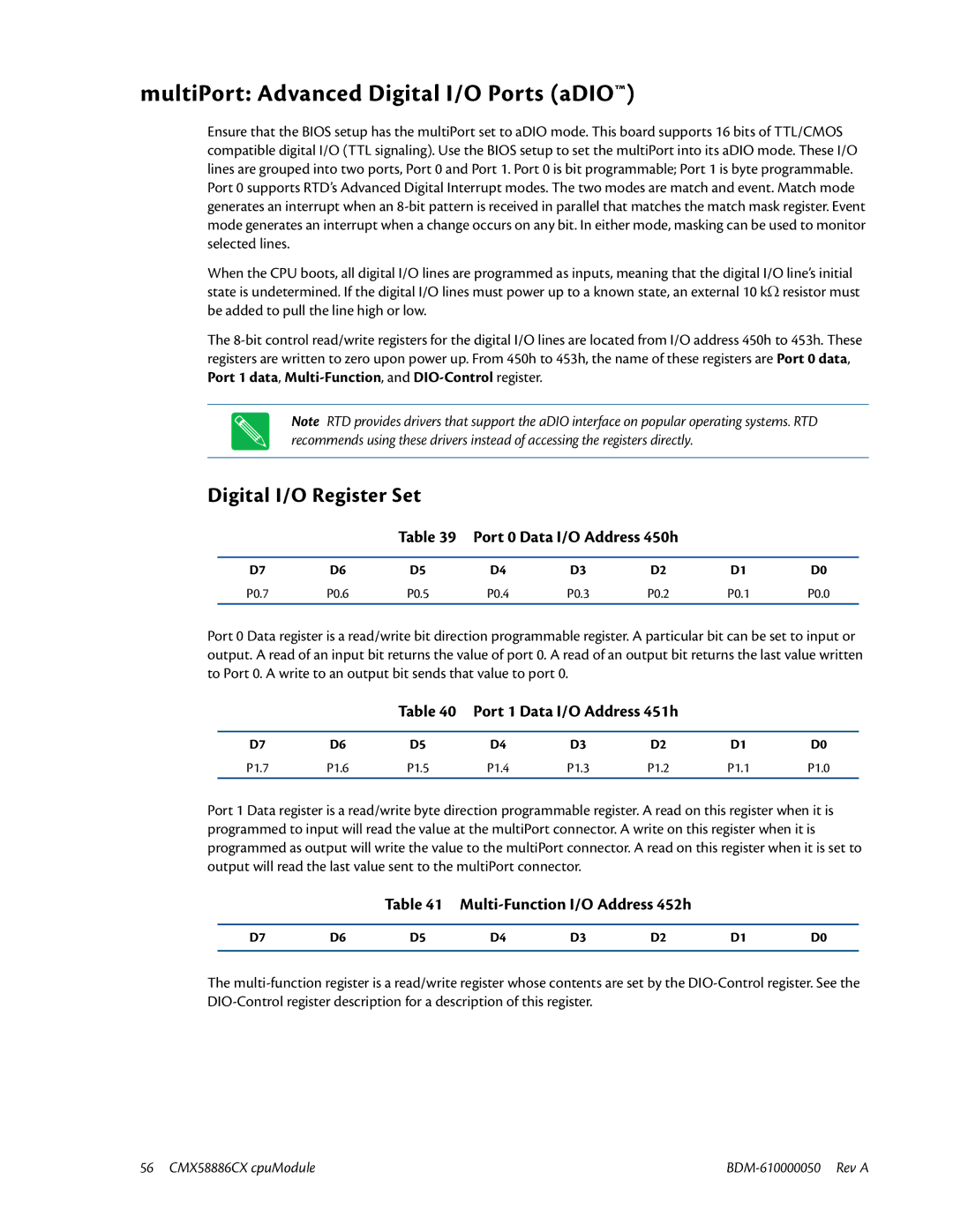
Table 39 Port 0 Data I/O Address 450h
D7 | D6 | D5 | D4 | D3 | D2 | D1 | D0 |
P0.7 | P0.6 | P0.5 | P0.4 | P0.3 | P0.2 | P0.1 | P0.0 |
|
|
|
|
|
|
|
|
Port 0 Data register is a read/write bit direction programmable register. A particular bit can be set to input or output. A read of an input bit returns the value of port 0. A read of an output bit returns the last value written to Port 0. A write to an output bit sends that value to port 0.
Table 40 Port 1 Data I/O Address 451h
D7 | D6 | D5 | D4 | D3 | D2 | D1 | D0 |
P1.7 | P1.6 | P1.5 | P1.4 | P1.3 | P1.2 | P1.1 | P1.0 |
Port 1 Data register is a read/write byte direction programmable register. A read on this register when it is programmed to input will read the value at the multiPort connector. A write on this register when it is programmed as output will write the value to the multiPort connector. A read on this register when it is set to output will read the last value sent to the multiPort connector.
Table 41 Multi-Function I/O Address 452h
D7 | D6 | D5 | D4 | D3 | D2 | D1 | D0 |
The
56 CMX58886CX cpuModule |