Block Diagram
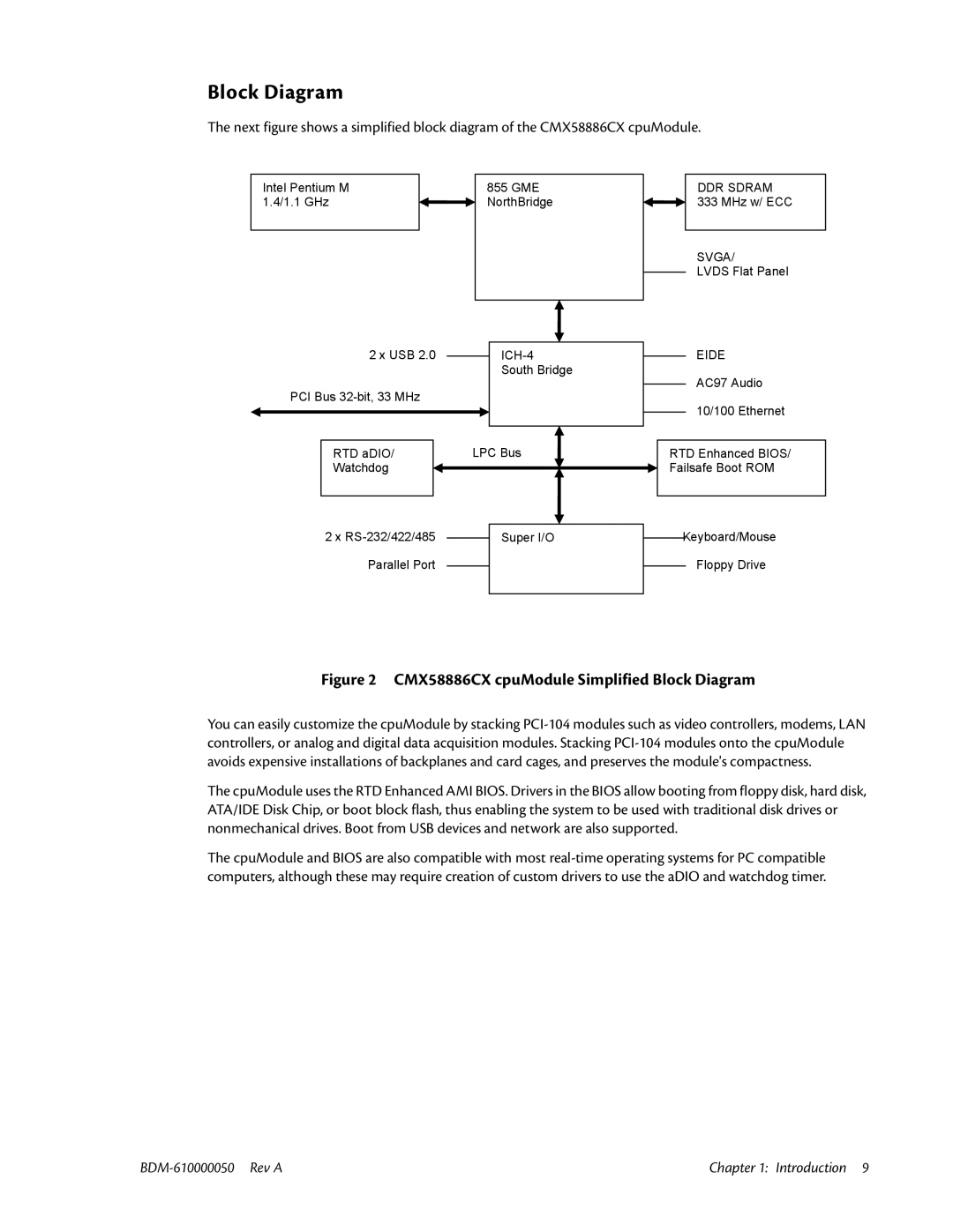
The next figure shows a simplified block diagram of the CMX58886CX cpuModule.
Intel Pentium M |
| 855 GME |
1.4/1.1 GHz |
| NorthBridge |
|
|
|
|
|
|
| 2 x USB 2.0 |
| ||
|
| |||
|
|
|
| South Bridge |
PCI Bus |
|
| ||
|
|
|
|
|
|
|
| LPC Bus | |
| RTD aDIO/ |
| ||
| Watchdog |
|
|
|
|
|
|
|
|
| 2 x |
|
| |
|
| Super I/O | ||
|
| |||
| Parallel Port |
|
| |
|
|
| ||
|
|
|
|
|
DDR SDRAM 333 MHz w/ ECC
SVGA/
LVDS Flat Panel
EIDE
AC97 Audio
10/100 Ethernet
RTD Enhanced BIOS/ Failsafe Boot ROM
Keyboard/Mouse
Floppy Drive
Figure 2 CMX58886CX cpuModule Simplified Block Diagram
You can easily customize the cpuModule by stacking
The cpuModule uses the RTD Enhanced AMI BIOS. Drivers in the BIOS allow booting from floppy disk, hard disk, ATA/IDE Disk Chip, or boot block flash, thus enabling the system to be used with traditional disk drives or nonmechanical drives. Boot from USB devices and network are also supported.
The cpuModule and BIOS are also compatible with most
Chapter 1: Introduction 9 |
