B1 | B3 | JP1 |
JP6
JP5
JP9
JP8
JP2
B2
B7
JP4
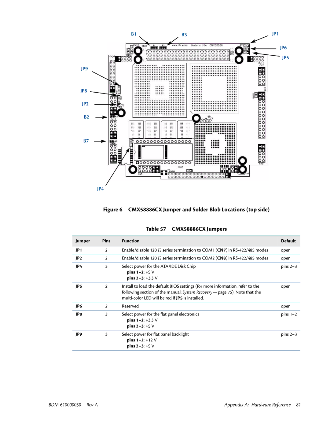
Figure 6 CMX58886CX Jumper and Solder Blob Locations (top side)
Table 57 CMX58886CX Jumpers
Jumper | Pins | Function | Default |
|
|
|
|
JP1 | 2 | Enable/disable 120 Ω series termination to COM1 (CN7) in | open |
|
|
|
|
JP2 | 2 | Enable/disable 120 Ω series termination to COM2 (CN8) in | open |
|
|
|
|
JP4 | 3 | Select power for the ATA/IDE Disk Chip | pins |
|
| pins |
|
|
| pins |
|
|
|
|
|
JP5 | 2 | Install to load the default BIOS settings (for more information, refer to the | open |
|
| following section of the manual: System |
|
|
|
| |
|
|
|
|
JP6 | 2 | Reserved | open |
|
|
|
|
JP8 | 3 | Select power for the flat panel electronics | pins |
|
| pins |
|
|
| pins |
|
|
|
|
|
JP9 | 3 | Select power for flat panel backlight | pins |
|
| pins |
|
|
| pins |
|
|
|
|
|
Appendix A: Hardware Reference 81 |