Manuals
/
Intel
/
Computer Equipment
/
Computer Hardware
Intel
user manual
Connector Location on the AI5VG
Models:
AI5VG
1
24
57
57
Download
57 pages
62.48 Kb
21
22
23
24
25
26
27
28
Install
Signal Name Pin #
Password
Load Bios Defaults
Typematic Delay Msec
Bios Configuration
Reset Switch Pins 9
PCI#2 Access #1 Retry
Bios Setup
I/O Connectors
Page 24
Image 24
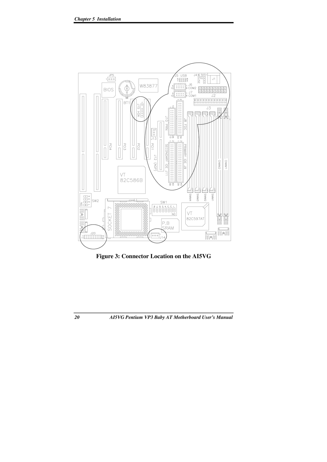
Chapter 5 Installation
Figure 3: Connector Location on the AI5VG
20
AI5VG Pentium VP3 Baby AT Motherboard User’s Manual
Page 23
Page 25
Page 24
Image 24
Page 23
Page 25
Contents
AI5VG
Page
Contents
Bios Configuration
Checklist
Introduction
Main Processor
L2 Cache
Main Memory
Memory Type
CPU Temperature Sensor
Onboard Bus Mastering Eide
Windows 95 Shut-Down
AGP Support Accelerated Graphics Port
Hardware Description
Layout of the AI5VG Motherboard
Processor and CPU Voltage
L2 Cache Memory
Bank0 Bank1 Total Memory
8MB
Bios
Bank0 DIMM2 Bank1 DIMM1 Total Memory
DMI Desktop Management Interface
ISA Plug and Play PnP Extension
Onboard CPU Temperature Sensor
Power Management
Onboard PCI Eide
Onboard Multi-I/O
I/O Port Address Map
DMA Channels
Address Device Description
Interrupt Request Lines IRQ
Accelerated Graphics Port AGP Slot
Level Function
Hardware Settings
Jumper Locations of the AI5VG
SW11-8 CPU Frequency Selector For Intel Pentium CPU
Bus Clock Mutiplier
For Cyrix 6x86, 6x86L CPU
SW21-4 CPU Voltage Selector
For Dual Voltage CPU Intel P55C, Cyrix 6x86L/MX, AMD K6
K6-233 35∝
JP5 Clear Cmos Selection
Installation
Connector Location on the AI5VG
I/O Connectors
J3 Pin # Description Wire Color
J2 ATX Power Supply Connector
J1, J4 AT Keyboard and PS/2 Mouse Connectors
Signal Name Pin #
J1 AT Keyboard Connector Pin # Signal Name
J8 Floppy Drive Connector
Pin # Signal Name
J7, J6 Serial Ports
RM/LC
J9, J11 Eide Connectors
J9 Primary IDE Connector Signal Name Pin #
J11 Secondary IDE Connector Signal Name Pin #
J10 Parallel Port Connector
J15 IrDA Connector
10 J5 USB Connector
USB USB+
11 J13 Wake on LAN Connector
12 J14 CPU Fan Power Connector
13 J20 Front Bezel Connector
Speaker Pins 1
J20 Pin # Signal Name
Power LED and Keylock Pins 11
ATX Power on Switch Pins 7
Reset Switch Pins 9
Bios Configuration
AGP
LANDesk User Guide
Bios Introduction
Bios Setup
Standard Cmos Setup
Standard Cmos Setup
Date
Mode for IDE HDD only Auto
Time
Primary HDDs / Secondary HDDs
LBA
Floppy 3 Mode Support
Drive a / Drive B
Video
Halt On
Bios Features Setup
Virus Warning
CPU Internal Cache / External Cache
Quick Power On Self Test
Boot Sequence
Boot Up Floppy Seek
Boot Up NumLock Status
Typematic Rate Setting
Typematic Delay Msec
Video Bios Shadow
Typematic Rate Chars/Sec
Chipset Features Setup
Video Bios Cacheable
System Bios Cacheable
Cache Timing
Memory Hole at 15MB Addr
Power Management Setup
IRQ4 COM1
HDD Power Down
Doze Mode
Suspend Mode
PM Control by APM
PM Events
PNP/PCI Configuration
PNP OS Installed
Reset Configuration Data
Resources Controlled by
PCI Delay Transaction
PCI#2 Access #1 Retry
CPU to PCI Write Buffer
PCI Dynamic Bursting
PCI IDE IRQ Map To
Load Bios Defaults
Load Setup Defaults
IDE Prefetch Mode
IDE HDD Block Mode
Integrated Peripherals
OnChip Primary/Secondary PCI IDE
Uart 2 Mode
Onboard Parallel Mode
IDE Primary/Secondary Master/Slave Udma
Onboard FDD Controller
Supervisor / User Password
Supervisor Password
IDE HDD Auto Detection
HDD Low Level Format
Save & Exit Setup
Exit Without Saving
Top
Page
Image
Contents