8355
8355 N/B Maintenance
Contents
Trouble Shooting ………………………………………………………………………………………
Audio Failure ………….……………………………………………………………………………………………
Hardware Engineering Specification
Introduction
8355 N/B Maintenance
System Hardware Part
CPU
CPU ClawHammer Processor
Compatible with Existing 32-bit Code Base
AMD x86-64 Technology
Integrated Memory Controller
Power Management
HyperTransport. Technology to I/O Devices
Kbyte 2-way Associative ECC-Protected L1 Data Cache
Way Associative ECC-Protected L2 Cache
Packaging
Power Supplies
Electrical Interfaces
System frequency
System frequency synthesizerICS950402
Programmable Timing Control Hub AMD-K8 processor
Recommended Application
Features
High Performance K8 CPU Interface
VIA K8T800+VT8235
3.1 K8T800
Full Featured Accelerated Graphics Port AGP 8x Controller
8355 N/B Maintenance
3.2 VT8235
8355 N/B Maintenance
General Description
Smartshader Advanced Shader Technology
High Performance Memory Support
Dual Display Support
Ideal for Windows 2000 and Windows XP
General and Interfacing Features
8355 N/B Maintenance
8355 N/B Maintenance
5 AC’97 Audio System C-MEDIA Electronics INC., CMI9738-S
8355 N/B Maintenance
MDC PCTel Modem Daughter Card PCT2303W
Operating System Compatibility
Compatibility
Modulation
Error Correction
Dtmf signal level
Data Compression
DTE interface Dtmf Tone Frequency
High group 10+/-2dBm Low group 12+/-2dBm
Transmit Level
Integrated 400 Mbit 2-Port PHY
7 VT6307L PCI 1394a Integrated Host Controller
Overview
8355 N/B Maintenance
Main Features
Embedded CONTROLLER-H8
Interface
Timer
Memory
Converter
Ports
Power-down modes
Other features
Interrupts
Wait control
Features
64MB, 128MB, 256MB, 512MB x64 200-Pin DDR Sdram SODIMMs
System Flash Memory Bios
Memory System
11 VT6103 Fast Ethernet 10/100 1-PORT PHY/TRANSCEIVER
Cardbus/MediaReader Controller
3V operation with 5V tolerant
Smart Card Interface
Pin Lqfp / 209-ball Lfbga package for CB710 PCI Interface
CardBus Interface
Secure Digital Interface
Memory Stick Interface
Interrupt configuration
Power Management Control Logic
Stick interface
SmartMedia Interface
Supports Zoomed Video port Power Switch Interface
Misc Control Logic
General Description
Outstanding Features
SuperI/O-PC87393
8355 N/B Maintenance
Hot Key Function
Keys Feature Meaning Combination
Other Functions
Power ON/OFF/Suspend/Resume Button
Cover Switch
APM mode
Acpi mode
LED Indicators
Fan power on/off management
Cmos Battery
7 I/O Port
Mini PCI type III BBattery current limit and learning
Peripheral Components
ROM Drive
Power Management
System Management Mode
Full on mode
Doze Mode
Suspend to Dram
Suspend to HDD
Other Power Management Functions
HDD & Video Access
Appendix 1 VT 8235 Gpio Definition
To the previous table
Appendix 2 H8 Pins Definition
Shadowed block is the selected function
Charging
KB OUT8
Ilimit
↑ Pull High ↓ Pull Low →3V Level shift
Appendix 3 8355 product spec
CPU
AC adapter
FCC, CE, UL, TUV, CB, Bsmi
System View and Disassembly
System View
Front View
Left-side View
Right-side View
Rear View
Bottom View
Top View
System Disassembly
DDR Sdram
Reassembly
Battery Pack
Disassembly
Keyboard
Remove three screws
Slide out the keyboard cover
Disconnect the cable from system board. Figure
3 CPU
Remove four screws
Disconnect the fan’s cord
HDD Module
11 Remove HDD compartment
13 slide out the hard disk drive
5 CD/DVD-ROM Drive
15 Remove the CD/DVD -ROM drive
SO-DIMM
16 Remove the SO-DIMM
LCD Assembly
17 Remove two screws
19 Remove the hinge cover
21 Remove the LCD assembly
Inverter Board
22 Unscrew four screws
8355 N/B Maintenance
LCD Panel
24 Separate the LCD panel
8355 N/B Maintenance
System Board
26 Unscrew nine screws
28 Remove the top cover
Unscrew one screw and disconnect fan’s cord. Figure
Reassembly
Modem Card
32 Remove the modem card
Touch Pad
33 Free the touch pad
8355 N/B Maintenance
Definition & Location of Connectors / Switches
Main Board Side a
Definition & Location of Connectors/ Switches
VR1 Volume Controller
Main Board Side B
Definition & Location of Major Components
U517 TPA0202 Audio Amplifier U518 CMI9738 Audio Codec
Pin Descriptions of Major Components
AMD Athlontm 64 Processor-1
DDR Sdram Memory Interface
DDR Sdram Memory Interface Continue
AMD Athlontm 64 Processor-2
HyperTransport Technology
Debug
Miscellaneous
Hyper Transport Receive Interface
K8T800MVT8385 North Bridge-1
Hyper Transport transmit Interface
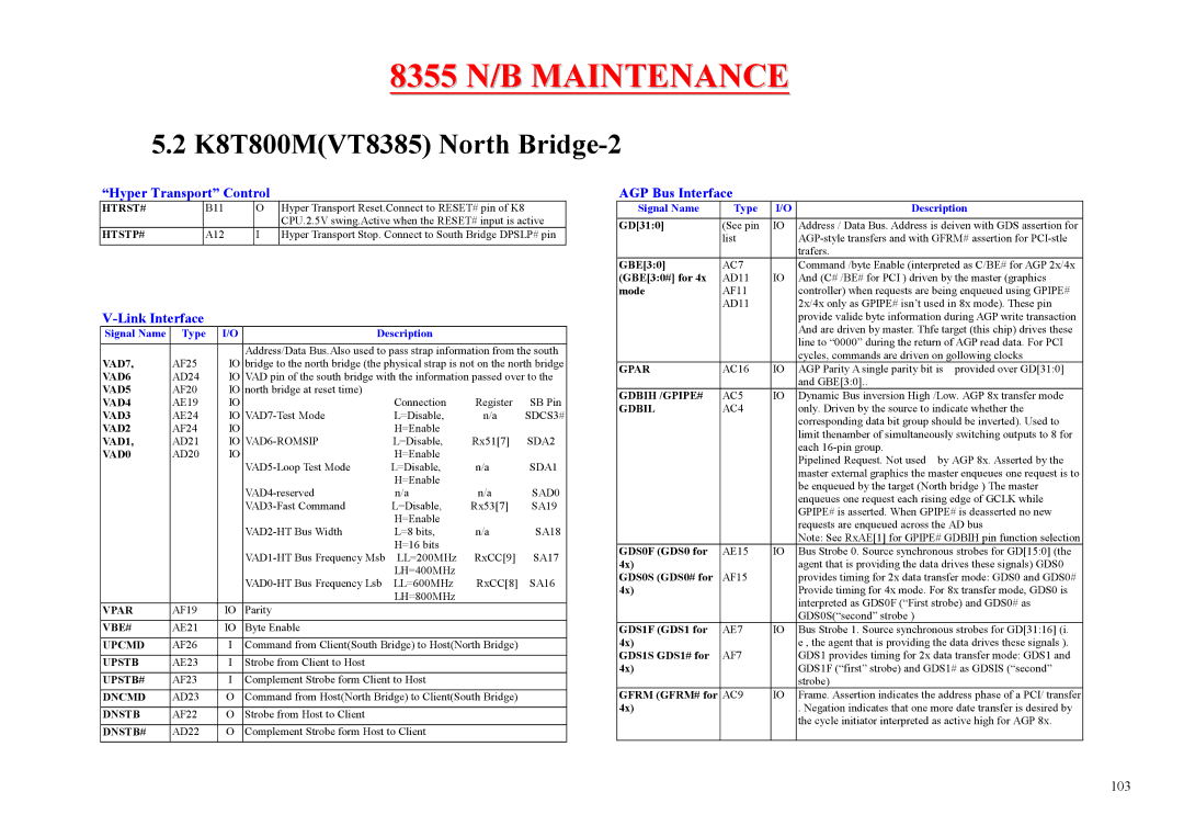
K8T800MVT8385 North Bridge-2
Hyper Transport Control
Link Interface
AGP Bus Interface
K8T800MVT8385 North Bridge-3
Girdy GIRDY#
Clock, Reset, Power Control and Test
K8T800MVT8385 North Bridge-4
Straps
VT8235 South Bridge-1
Advanced Programmable Interrupt Controller APICInterface
VT8235 South Bridge-2
CPU Speed Control Interface
Low Pin Count LPCInterface
CPU Interface
PCI Bus Interface Continue
VT8235 South Bridge-3
PCI Bus Interface
VT8235 South Bridge-4
LAN Controller -Media Independent Interface MII
General Purpose I/O
Universal Serial Bus 2.0 Interface
VT8235 South Bridge-5
UltraDMA-133 /100 /66 /33 Enhanced IDE Interface
UltraDMA-133 /100 /66 /33 Enhanced IDE Interface Continue
Serial IRQ
Resets,Clocks,and Power Status
VT8235 South Bridge-6
General Purpose Inputs
General Purpose Inputs Continue
VT8235 South Bridge-7
Power Management and Event Detection
Power Management and Event Detection Continue
Power and Ground
VT8235 South Bridge-8
Internal Keyboard Controller
AC97 Audio /Modem Interface
Power and Ground Continue
ISA Subset /Parallel Bios ROM Interface
VT8235 South Bridge-9
System Management Bus SMBInterface I 2 CBus
U506
System Block Diagram
U503
Maintenance Diagnostics
Error Codes
Code Post Routine Description
118
Diagnostic Tool for Mini PCI Slot
Debug Tool
Diagnostic Tool for PIO Port
Trouble Shooting
No Power
+1.25VSREFMEM
+1.2VLDTA Agpvddq
PJ502
No power
Battery Can not Be Charged
Adinp
Battery can not Charge
No Display
System Clock Check
Reset Circuit Checking1
No Display System Failure
Reset Circuit Checking2
No Display System Failure
Parts Signals
No Display
AGP Controller Failure LCD No Display
U9 P6
AGP Controller Failure
Charge BD J2,J3 are cold colder?
External Monitor No Display
J503
Display Yes OK? Replace faulty monitor
Memory Test Error
Symptom The extend DDR RAM is failure or system hangs up
Memory Test Error
Parts
Keyboard K/B Touch-Pad T/P Test Error
Key Board Controller
Keyboard or Touch-Pad Test Error
Test Yes Ok? Replace the faulty Keyboard or Touch-Pad
Hard Disk Driver Test Error
Hard Disk Driver Test Error
Hard Driver Test Error
CD-ROM Driver Test Error
J530
CD-ROM Driver Test Error
USB Test Error
Symptom An error occurs when a USB I/O device is installed
U501
USB Test Error
PartsSignals
Symptom An error occurs when a PC card device is installed
PC-Card Socket Failure
PC Card Test Error
Memory-Card Socket Failure
Memory Card Test Error
Memory-Card Socket Failure
IEEE1394 Test Error
Symptom An error occurs when IEEE1394 device is installed
Test Error
LAN Test Error
Symptom An error occurs when LAN device is installed
LAN Test Error
Correct it
Audio Failure
Input Of Audio Subsystem
Output Of Audio Subsystem
Audio Drive Failure
Spare Part List-1
Part Number Description LocationS
Spare Part List-2
Spare Part List-3
CFM-BATFUSE Thermal 98C
Spare Part List-4
DIODEBAV70LT1,70V,225MW,SOT-23
Spare Part List-5
DVD Combo DRIVE8X24X10X24X,SBW
Spare Part List-6
ICEM6A9320BI-3.6M,DDR SDRAM,4MX
Spare Part List-7
ICVT8235,SOUTH BRIDGE,BGA,487P
LABELSOFTWARE,INSYDE BIOS-M
Spare Part List-8
Spare Part List-9
RELAYREED,200V,.5A,NORMAL Open SW1
Spare Part List-10
RES2M
Spare Part List-11
RP7,RP8
Spare Part List-12
RP6,RP9
Spare Part List-13
TRANSDTC144WK,NPN,SOT-23,SMT
WIRE#28,UL1061,40MM,BLUE,PRC
Spare Part List-14
Page
Page
Model
CPURESET# CPURESET# 3,12 DDRRASB#
Memresetl
CPURESET#
Corefbh
NBLDTRST# CPURESET#
VID0
VID1
VID2
DIMM-SLOT & Termination
K8T400M- VT8385
FS0 14MSBIOSC
H8RESET#
ACPOWER#
H8RESET# BATTG#
AGPRESET#
M10GPIO0
M10GPIO4
M10GPIO5
ATI M10-P2/4
MEMAMD2
MEMAMA2
MEMAMD0
VMDA0 MEMAMD0
VMA0
VMDA0 VMA0
VMB0 VMDB0 VMDB32 VMA1 VMDA1 VMDA33
VMA2
Crtin
Crtgreen
+PANELVDD
PANELID0 PANELID2 PANELID3
VT8235 1/3- PCI & USB
VT8235 2/3- IDE & AC97
VT8235 3/3- VLINK&LAN
IDEDPDD0
IDEDPDD1 HDPDD2
IDEDPDD2
HDPDD3 IDEDPDD3 HDPDD4
CAD11 CVS1 CARDRESET#
POWERONRESET#
CAD1
CAD2
MINIPCIGPORESET#
Wirelesspd
SDCD# GND SDWP#
SDWP# SDDATA1 LEDCL190 SDDATA0 Sdclk Sdcmd SDDATA3 SDDATA2
PCIAD4 PCIAD1
TPA0N
TPA0P
TPB0P
LANPHYRESET#
LANMRXDV2
PJTX+
LANTX+
Avdd Micvref
Micint
Micext AC97SDOUT
AC97SDIND0
Audiomute Ampmute
DEVICEDECT#
DECTHP#/OPT
Spdifout
LPCSPIORESET# PD6
LPCSPIORESET# LPCFRAME#
INIT#
PIOD/INT#
Tclkd H8RESET#
SCI#/FANSWITCH H8WAKEUP#
H8ENABKL H8RESET#
SCI#/FANSWITCH
USBOC0# USBOC2#
USBOC5# USBOC2#
USBP0P
USBP2P
SA0 SD1 SA1
SD2 SA2 PCIGNT#4 SD3 SA3 PCIGNT#5 PCICARDBUSGNT#0
SD4 SA4
SD6 SA6
OD3
OD5
Pgvcccore
PWRONM9
+2.5VS&+1.25VS&+1.8V&+1.2V
+3VS / +5VS
DVMAINP2
VOSENSE1
VOSENSE2
For M10 +1.2V&+1.0V
Adinp
ADP1
Batt
Ilimit
Adinp Batt
Liovp
Liovp Charging
Battdead
VMAINP3
PVID0
PVID1
PVID2
Reference Material
Tel Fax Second Edition Nov Mail Willy .Chen @ mic.com.tw