MODELS:
Using Lead Free Solder
The symbol shown below indicates Lead (Pb) Free |
| • Poor |
| ||||
solder was used during the construction of PWBs. |
| • Higher temperatures can cause flux spattering. | |||||
Only Lead Free solder should be used when servic- | • Soldering iron tip life is shortened. |
| |||||
ing these PWBs. |
|
| • Dull finish solder joints (not shiny) can appear to be | ||||
Solder must be compatible with that used by the |
| a “cold” solder joint. |
|
| |||
|
|
|
|
|
| ||
manufacturer. Leaded solder can not be used on |
| In general a tip temperature of 700° F will usually provide | |||||
PWBs manufactured with | good results. |
|
|
|
| ||
ishi standard for service requires the use of |
|
|
|
|
| ||
Copper | Displays used to indicate | ||||||
through the Parts Department. |
|
| |||||
Order part number: PB FREE SOLDER |
|
| PCBs will be marked, indicating the level of | ||||
|
|
| struction. Table 1 defines the levels by phase and shows | ||||
Lead Free solder has a higher melting point, and does | the different symbols that will be displayed on the PCB. | ||||||
not “wet” as well as leaded solder. This means it does | Additionally, a PCB constructed using | ||||||
not adhere as readily to the solder iron tip, and the |
| be simply marked LFS. |
|
| |||
surface to be soldered. To counteract this, the flux |
| When possible, the indication will be placed close to the | |||||
used is more corrosive. |
|
| |||||
|
|
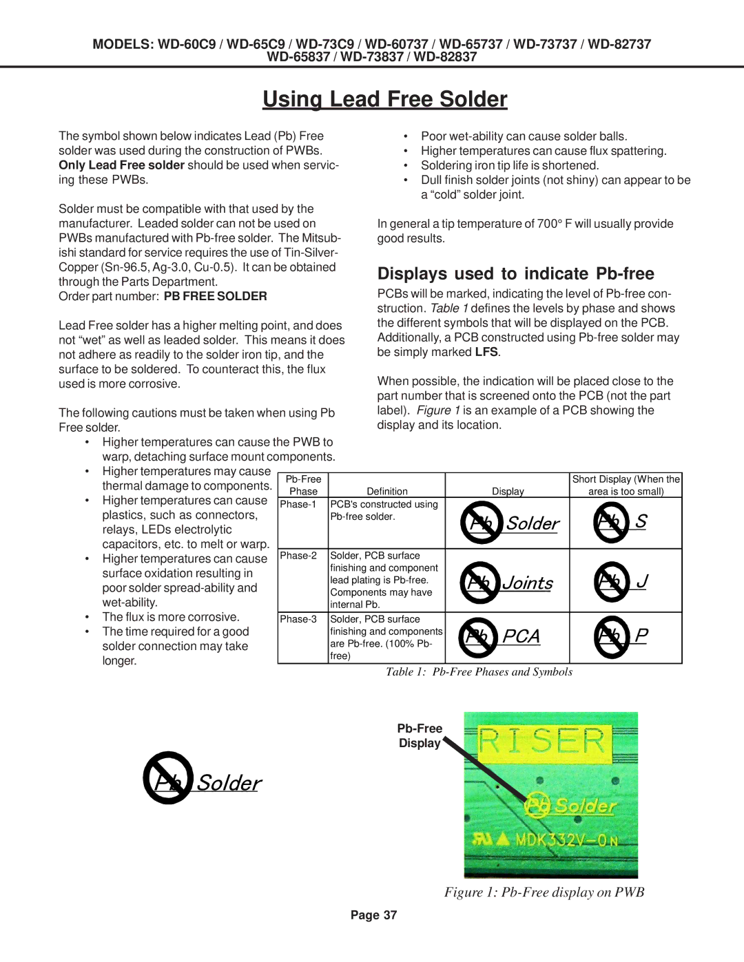
| part number that is screened onto the PCB (not the part | ||||
The following cautions must be taken when using Pb | label). Figure 1 is an example of a PCB showing the | ||||||
Free solder. |
|
| display and its location. |
|
| ||
• Higher temperatures can cause the PWB to |
|
|
|
|
| ||
warp, detaching surface mount components. |
|
|
|
|
| ||
• Higher temperatures may cause |
|
|
|
| Short Display (When the | ||
thermal damage to components. |
|
|
|
| |||
Phase |
| Definition |
| Display | area is too small) | ||
• Higher temperatures can cause |
|
| |||||
PCB's constructed using |
|
|
|
| |||
plastics, such as connectors, |
| Pb | Solder | Pb | S | ||
relays, LEDs electrolytic |
|
|
| ||||
|
|
|
|
|
|
| |
capacitors, etc. to melt or warp. | Solder, PCB surface |
|
|
|
| ||
• Higher temperatures can cause |
|
|
|
| |||
surface oxidation resulting in |
| finishing and component | Pb | Joints | Pb | J | |
| lead plating is | ||||||
poor solder |
| ||||||
| Components may have |
|
|
|
| ||
| internal Pb. |
|
|
|
| ||
• The flux is more corrosive. | Solder, PCB surface |
|
|
|
| ||
• The time required for a good |
| finishing and components | Pb | PCA | Pb | P | |
solder connection may take |
| are |
|
|
|
| |
longer. |
| free) |
|
|
|
|
|
Table 1:
Display
Pb Solder
Figure 1: Pb-Free display on PWB
Page 37