ADHFI Status bit of ADC FIFO
with more than 255 samples.
0 = Indicates an ADC
ADNEI Status bit of ADC FIFO
1 = Indicates an ADC FIFO
0 = Indicates an ADC FIFO
ADNE
1 = Indicates ADC FIFO has at least one word to be read. 0 = Indicates ADC FIFO is empty.
LADFUL Status bit of ADC FIFO FULL status. This bit is latched.
1 = Indicates the ADC FIFO has exceeded full state. Data may have been lost. 0 = Indicates
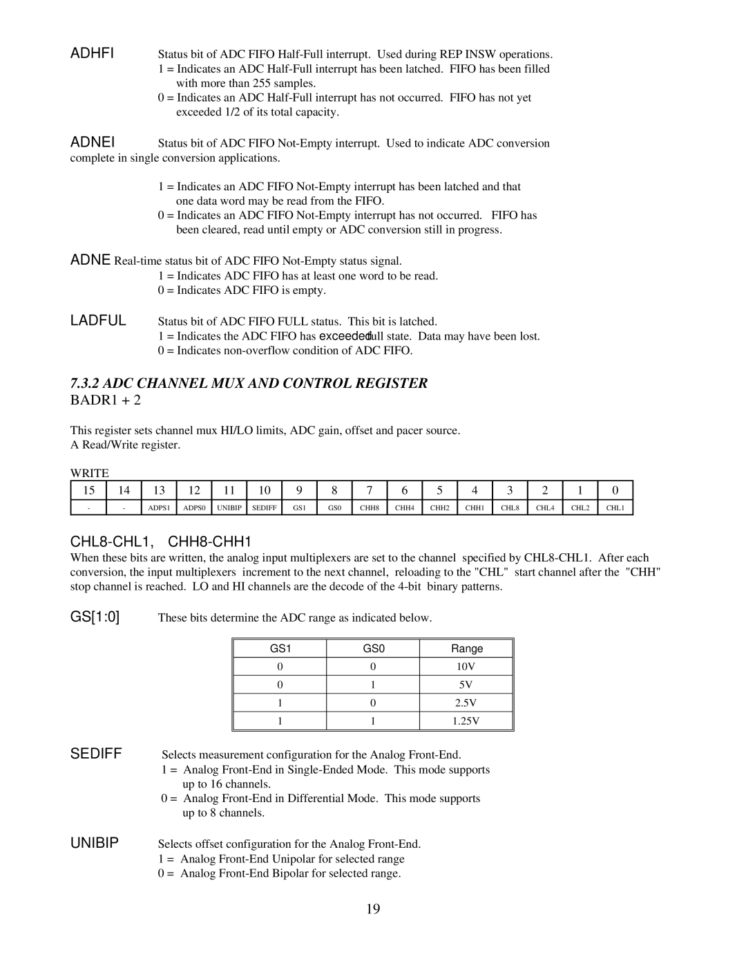
7.3.2ADC CHANNEL MUX AND CONTROL REGISTER BADR1 + 2
This register sets channel mux HI/LO limits, ADC gain, offset and pacer source.
A Read/Write register.
WRITE
15 | 14 | 13 | 12 | 11 | 10 | 9 | 8 | 7 | 6 | 5 | 4 | 3 | 2 | 1 | 0 |
|
|
|
|
|
|
|
|
|
|
|
|
|
|
|
|
- | - | ADPS1 | ADPS0 | UNIBIP | SEDIFF | GS1 | GS0 | CHH8 | CHH4 | CHH2 | CHH1 | CHL8 | CHL4 | CHL2 | CHL1 |
|
|
|
|
|
|
|
|
|
|
|
|
|
|
|
|
CHL8-CHL1, CHH8-CHH1
When these bits are written, the analog input multiplexers are set to the channel specified by
GS[1:0] These bits determine the ADC range as indicated below.
GS1 | GS0 | Range |
|
|
|
0 | 0 | 10V |
|
|
|
0 | 1 | 5V |
|
|
|
1 | 0 | 2.5V |
|
|
|
1 | 1 | 1.25V |
|
|
|
|
|
|
SEDIFF Selects measurement configuration for the Analog
1 = Analog
0 = Analog
UNIBIP Selects offset configuration for the Analog
0 = Analog
19