![]()
![]()
![]() X7DA3+ User's Manual
X7DA3+ User's Manual
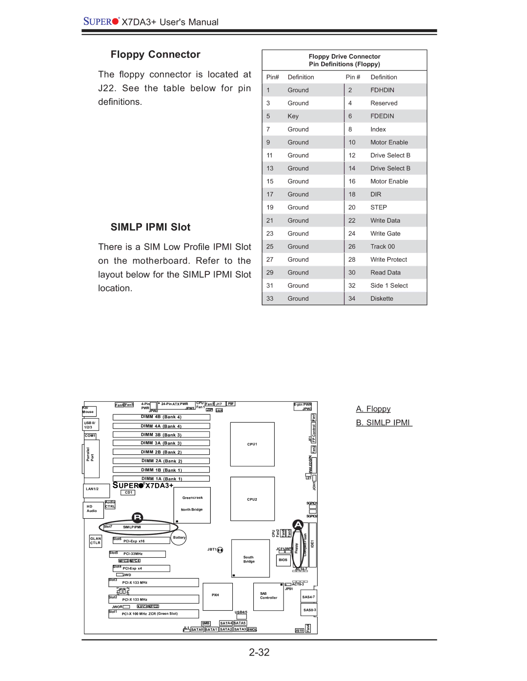
Floppy Connector
Floppy Drive Connector Pin Definitions (Floppy)
The fl oppy connector is located at J22. See the table below for pin defi nitions.
SIMLP IPMI Slot
There is a SIM Low Profi le IPMI Slot on the motherboard. Refer to the layout below for the SIMLP IPMI Slot location.
Pin# Defi nition
1Ground
3Ground
5Key
7Ground
9Ground
11 Ground
13 Ground
15 Ground
17 Ground
19 Ground
21 Ground
23 Ground
25 Ground
27 Ground
29 Ground
31 Ground
33 Ground
Pin # Definition
2FDHDIN
4Reserved
6FDEDIN
8Index
10Motor Enable
12Drive Select B
14Drive Select B
16Motor Enable
18DIR
20STEP
22Write Data
24Write Gate
26Track 00
28Write Protect
30Read Data
32Side 1 Select
34Diskette
KB/ Mouse
USB 0/ 1/2/3
COM1
Parrallel PortJLAN1
| Fan6 | Fan5 |
| CPU | Fan7 | J17 | PSF | ||||
|
|
| PWR |
| JPW1 | Fan 1 | J3P | JAR | |||
|
|
| JPW2 |
|
|
| |||||
|
|
| DIMM 4B (Bank 4) |
|
|
|
|
|
| ||
|
|
|
|
|
|
|
|
|
|
|
|
|
|
| DIMM 4A (Bank 4) |
|
|
|
|
|
| ||
|
|
|
|
|
|
|
|
|
| ||
|
|
| DIMM 3B (Bank 3) |
|
|
|
|
|
| ||
|
|
|
|
|
|
|
|
|
| ||
|
|
| DIMM 3A (Bank 3) |
|
|
|
|
|
| ||
|
|
|
|
|
|
|
|
|
| ||
|
|
| DIMM 2B (Bank 2) |
|
|
|
|
|
| ||
|
|
|
|
|
|
|
|
|
| ||
|
|
| DIMM 2A (Bank 2) |
|
|
|
|
|
| ||
|
|
| DIMM 1B (Bank 1) |
|
|
|
|
|
| ||
CPU1
| |
JPW3 |
|
|
|
| Fan1 |
|
|
F1J | FP Control |
|
|
| Fan2 |
PWLEDSPK |
|
|
A.Floppy
B.SIMLP IPMI
LAN1/2
HD
Audio
GLAN
CTLR
|
|
|
|
|
|
|
|
|
|
| DIMM 1A (Bank 1) | |||||||||
| SUPER | X7DA3+ |
|
|
| |||||||||||||||
| ||||||||||||||||||||
|
| |||||||||||||||||||
|
|
|
|
|
| CD1 |
|
|
|
|
|
|
|
|
|
|
|
|
| |
|
|
|
|
|
|
|
|
|
|
|
|
|
|
|
|
|
|
| Greencreek | |
Audio |
|
|
|
|
|
|
|
|
|
|
|
|
|
|
|
|
|
| ||
|
|
|
|
|
|
|
|
|
|
|
|
|
|
|
| |||||
CTRL |
|
|
|
|
|
|
|
|
|
|
|
|
|
|
|
| North Bridge | |||
|
|
|
|
|
|
|
| B |
|
|
|
|
|
|
| |||||
|
|
|
|
|
|
|
|
|
|
|
|
|
|
|
|
| ||||
|
|
|
|
|
|
|
|
|
|
|
|
|
|
|
|
| ||||
Slot7 |
| SIMLPIPMI |
|
|
|
|
|
|
|
|
| |||||||||
|
|
|
|
|
|
|
|
|
|
|
|
|
|
| ||||||
|
|
|
|
|
|
|
|
|
|
|
|
|
|
|
|
| Battery | |||
|
|
|
|
|
|
|
|
|
|
|
|
|
|
|
|
| ||||
|
| Slot6 |
|
|
|
|
|
|
|
| ||||||||||
|
|
|
|
|
|
|
|
|
|
|
|
| ||||||||
|
|
|
|
|
|
|
|
|
|
|
|
|
|
|
|
|
|
|
|
|
| Slot5 |
|
|
|
|
|
|
|
|
|
| |||||||||
|
|
|
|
|
|
|
|
|
|
|
|
|
|
| ||||||
|
|
|
|
|
|
|
|
|
|
|
|
|
|
|
|
|
|
|
|
|
|
|
|
|
| 2 | C3 |
| 2 | C4 |
|
|
|
|
|
|
|
|
|
| |
|
|
|
| JI | JI |
|
|
|
|
|
|
|
|
|
| |||||
|
|
|
|
|
|
|
|
|
|
|
|
|
|
|
|
|
|
|
|
|
|
| Slot4 |
|
|
|
|
|
|
|
|
|
| ||||||||
|
|
|
|
|
|
|
|
|
|
|
|
|
|
| ||||||
|
|
|
|
|
|
|
|
|
|
|
|
|
|
|
|
|
|
|
|
|
|
|
|
|
|
| JWD |
|
|
|
|
|
|
|
|
|
|
|
|
| |
|
|
|
|
|
|
|
|
|
|
|
|
|
|
|
|
|
|
|
|
|
| Slot3 |
|
|
|
|
|
|
| ||||||||||||
|
|
| JPL1 |
| JPL2 |
|
|
|
|
|
|
|
|
|
|
|
|
| ||
| Slot2 | 133 MHz |
|
|
|
|
|
|
| |||||||||||
|
|
|
|
|
|
|
|
|
|
|
| |||||||||
|
|
|
|
|
|
|
|
|
|
|
|
|
|
|
|
|
|
|
|
|
|
|
|
|
|
|
|
|
|
| 2 | C1 | 2 | C2 |
|
|
|
|
|
| |
| JWOR |
|
|
|
| JI | JI |
|
| |||||||||||
|
|
|
|
|
|
|
|
|
|
|
|
|
|
|
|
|
|
|
|
|
| Slot1 | 100 MHz ZCR (Green Slot) |
| |||||||||||||||||
|
|
|
|
|
| |||||||||||||||
|
|
|
|
|
|
|
|
|
|
|
|
|
|
|
|
|
|
|
|
|
JBT1![]()
PXH
|
|
|
|
|
|
|
|
|
|
| LE1 |
| ||
|
|
|
|
|
|
|
|
|
|
|
|
|
| JOH1 |
|
|
| CPU2 |
|
|
|
|
| SGPIO1 | |||||
|
|
|
|
|
|
|
|
|
|
|
| |||
|
|
|
|
|
|
|
|
|
|
|
|
|
|
|
|
|
|
|
|
|
|
|
|
|
|
|
|
|
|
|
|
|
|
|
|
|
|
|
|
|
| SGPIO2 | ||
|
|
|
|
|
|
|
|
|
| A |
|
|
|
|
|
|
|
|
| CPU Fan2 |
|
|
|
|
|
| |||
|
|
|
|
|
|
|
|
|
|
| ||||
|
|
|
|
| Fan8 | Fan3 |
| Flash |
| DE1 | ||||
|
|
|
|
|
|
|
|
|
|
|
| |||
|
|
|
|
|
|
|
|
|
| Floppy | Compact |
| ||
|
|
|
|
|
| JCF1JWF1 |
|
|
| I | ||||
|
| South |
|
|
|
|
|
|
|
|
|
| ||
|
|
|
|
|
|
|
|
|
|
|
| |||
|
|
|
|
| BIOS |
|
|
|
|
| ||||
|
| Bridge |
|
|
|
|
|
|
|
| ||||
|
|
|
|
|
|
|
|
|
|
|
| |||
|
|
|
|
|
|
|
|
|
|
|
|
|
| |
|
|
|
|
|
|
|
|
|
| |||||
|
|
|
|
|
|
|
|
|
|
|
|
| ||
|
|
|
|
|
|
|
|
|
|
|
|
| ||
|
|
|
| SAS |
| JPS1 |
|
|
|
|
| |||
|
|
|
|
|
|
| ||||||||
|
|
|
| Controller |
|
|
| |||||||
|
|
|
|
|
|
|
|
|
|
| ||||
|
|
|
|
|
|
|
|
|
|
|
|
| ||
|
|
|
|
|
|
|
|
|
|
|
|
| ||
|
|
|
|
|
|
|
|
|
|
| ||||
| USB4/5 |
|
|
| ||||||||||
|
|
|
|
|
|
|
| |||||||
|
|
|
|
|
|
|
|
|
|
|
|
|
|
|
|
|
|
|
|
|
|
|
|
|
|
|
|
|
|
|
|
| SMB |
| SATA4 | SATA5 |
|
|
|
|
|
|
|
|
| |
| JL1 |
|
|
|
|
|
|
|
|
|
| JS10 | Fan4 |
| ||
|
| SATA0 | SATA1 | SATA2 | SATA3 | JWOL |
|
|
|
|
|
|
|
| ||
|
|
|
|
|
|
|
|
|
|
|
|
|
|
|
|
|