![]()
![]()
![]()
![]()
![]() P8SC8/P8SCi User’s Manual
P8SC8/P8SCi User’s Manual
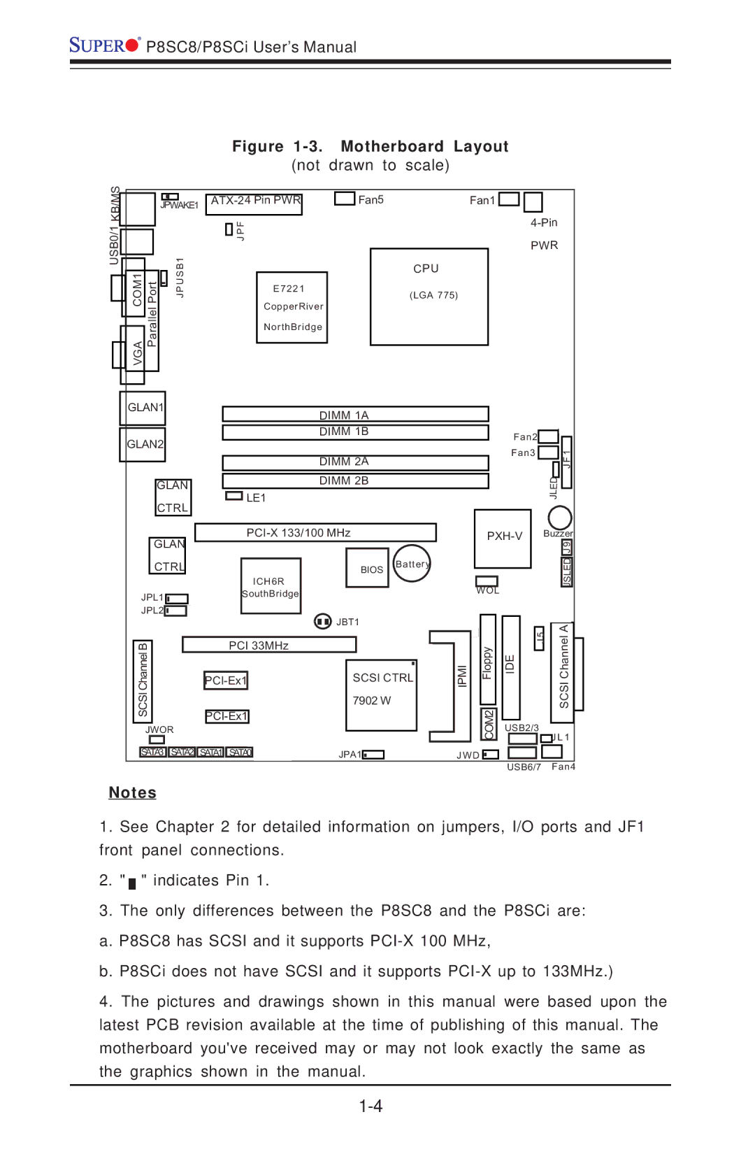
Figure 1-3. Motherboard Layout
(not drawn to scale)
USB0/1 KB/MS
VGA COM1 Parallel Port
JPWAKE1
B1
US
JP
| Fan5 | Fan1 | |
|
|
|
|
JPF |
|
| |
|
|
| CPU |
E7221 |
| (LGA 775) | |
|
|
| |
CopperRiver |
|
| |
NorthBridge |
|
| |
GLAN1 |
| DIMM | 1A |
|
|
|
| |
|
|
|
|
|
| |||
GLAN2 |
| DIMM | 1B | Fan2 |
|
|
| |
|
|
| ||||||
|
|
| ||||||
|
|
| ||||||
|
|
|
|
|
|
| ||
|
|
|
| Fan3 | 1 | |||
|
|
|
|
| ||||
|
| DIMM 2A |
|
|
| JF | ||
GLAN |
| DIMM 2B |
| JLED | ||||
CTRL |
| LE1 |
|
|
|
|
| |
|
|
|
|
|
| |||
|
|
|
|
|
|
|
| |
GLAN |
|
| Buzzer | |||||
|
|
|
|
| 9 | |||
|
|
|
|
|
|
|
| J |
CTRL
JPL1 ![]()
![]() JPL2
JPL2![]()
![]()
![]()
![]()
![]()
BChannel
SCSI
ICH6R
SouthBridge
PCI 33MHz
BIOS | Battery |
|
WOL
JBT1
JBT1 |
|
|
|
|
| Floppy | 5J |
SCSI CTRL | IPMI | IDE | |
| |||
7902 W |
|
|
|
D
E
L
JS
SCSI AChannel
JWOR |
|
|
SATA3 SATA2 | SATA1 | SATA0 |
JPA1 |
|
|
|
|
| COM2 | USB2/3 | ||
|
|
|
|
|
|
|
| ||
| JW D |
|
|
| |||||
|
|
|
| ||||||
|
|
|
|
|
|
| USB6/7 | ||
J L 1
Fan4
Notes
1.See Chapter 2 for detailed information on jumpers, I/O ports and JF1 front panel connections.
2." ![]() " indicates Pin 1.
" indicates Pin 1.
3.The only differences between the P8SC8 and the P8SCi are:
a. P8SC8 has SCSI and it supports
b. P8SCi does not have SCSI and it supports
4.The pictures and drawings shown in this manual were based upon the latest PCB revision available at the time of publishing of this manual. The motherboard you've received may or may not look exactly the same as the graphics shown in the manual.