Chapter 2: Installation
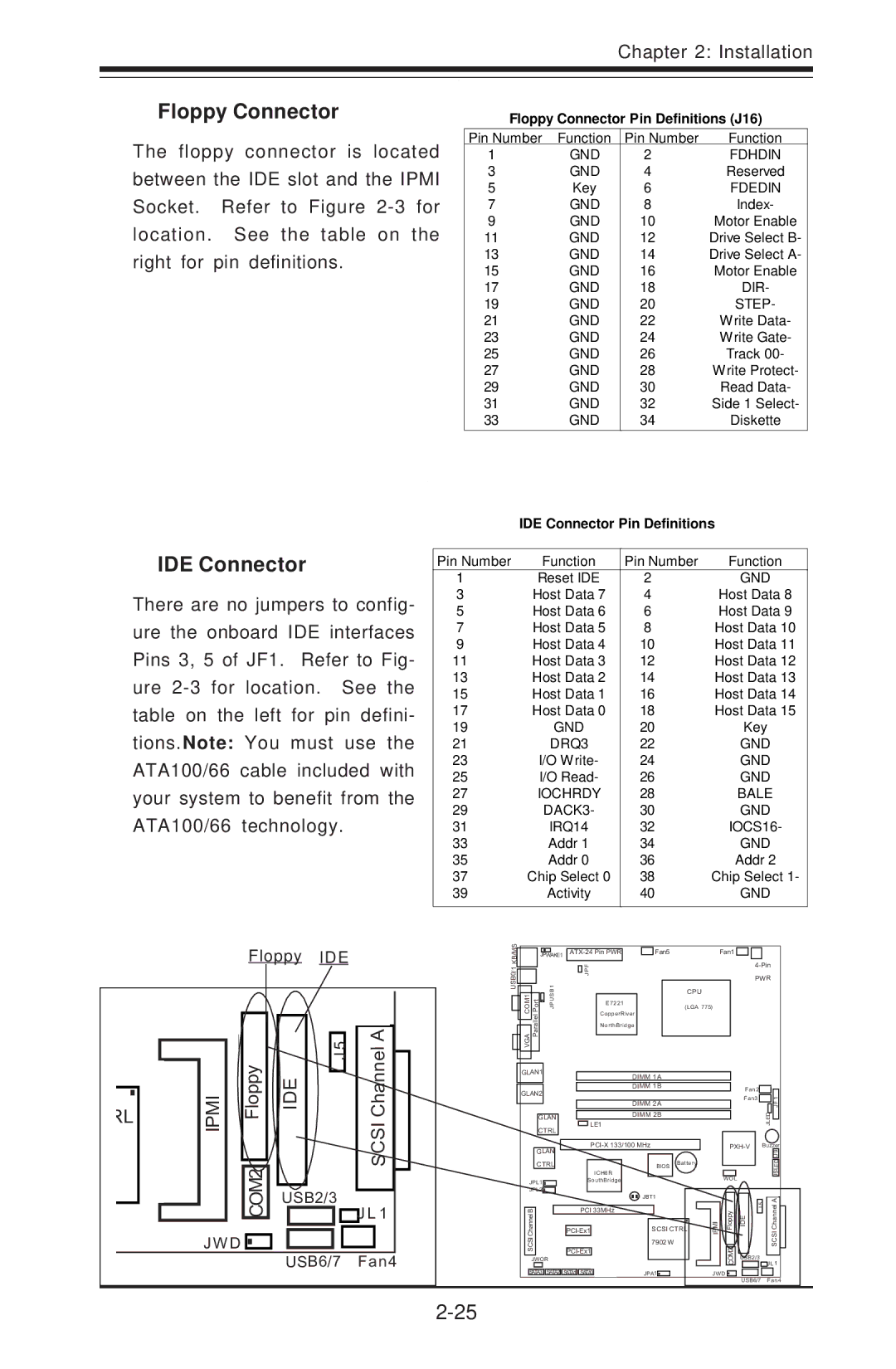
Floppy Connector
Floppy Connector Pin Definitions (J16)
The floppy connector | is located |
| Pin Number Function | Pin Number | Function | |||||||
| 1 | GND | 2 | FDHDIN | ||||||||
between the IDE slot and the IPMI |
| 3 | GND | 4 | Reserved | |||||||
| 5 | Key | 6 | FDEDIN | ||||||||
|
|
|
|
|
|
|
|
| ||||
Socket. | Refer | to | Figure | for |
| 7 | GND | 8 | Index- | |||
location. | See | the table | on | the |
| 9 | GND | 10 | Motor Enable | |||
| 11 | GND | 12 | Drive Select B- | ||||||||
right for | pin definitions. |
|
|
|
| 13 | GND | 14 | Drive Select A- | |||
|
|
|
| 15 | GND | 16 | Motor Enable | |||||
|
|
|
|
|
|
|
|
| ||||
|
|
|
|
|
|
|
|
| 17 | GND | 18 | DIR- |
|
|
|
|
|
|
|
|
| 19 | GND | 20 | STEP- |
|
|
|
|
|
|
|
|
| 21 | GND | 22 | Write Data- |
|
|
|
|
|
|
|
|
| 23 | GND | 24 | Write Gate- |
|
|
|
|
|
|
|
|
| 25 | GND | 26 | Track 00- |
|
|
|
|
|
|
|
|
| 27 | GND | 28 | Write Protect- |
|
|
|
|
|
|
|
|
| 29 | GND | 30 | Read Data- |
|
|
|
|
|
|
|
|
| 31 | GND | 32 | Side 1 Select- |
|
|
|
|
|
|
|
|
| 33 | GND | 34 | Diskette |
|
|
|
|
|
|
|
|
|
| IDE Connector Pin Definitions | ||
IDE Connector |
|
|
|
|
|
|
|
| ||||
|
|
| Pin Number | Function | Pin Number | Function | ||||||
|
|
|
| 1 |
| Reset IDE | 2 | GND | ||||
|
|
|
|
|
|
|
|
| ||||
There are no jumpers to config- |
| 3 |
| Host Data 7 | 4 | Host Data 8 | ||||||
| 5 |
| Host Data 6 | 6 | Host Data 9 | |||||||
|
|
|
|
|
|
|
|
| ||||
ure the onboard IDE interfaces |
| 7 |
| Host Data 5 | 8 | Host Data 10 | ||||||
Pins 3, 5 of JF1. | Refer to Fig- |
| 9 |
| Host Data 4 | 10 | Host Data 11 | |||||
| 11 | Host Data 3 | 12 | Host Data 12 | ||||||||
ure | See | the |
| 13 | Host Data 2 | 14 | Host Data 13 | |||||
| 15 | Host Data 1 | 16 | Host Data 14 | ||||||||
|
|
|
|
|
|
|
| |||||
table on | the left | for pin defini- |
| 17 | Host Data 0 | 18 | Host Data 15 | |||||
tions.Note: You | must | use | the |
| 19 | GND | 20 | Key | ||||
| 21 | DRQ3 | 22 | GND | ||||||||
ATA100/66 cable included with |
| 23 | I/O Write- | 24 | GND | |||||||
| 25 | I/O Read- | 26 | GND | ||||||||
|
|
|
|
|
|
|
| |||||
your system to benefit from the |
| 27 | IOCHRDY | 28 | BALE | |||||||
ATA100/66 technology. |
|
|
| 29 | DACK3- | 30 | GND | |||||
|
|
| 31 | IRQ14 | 32 | IOCS16- | ||||||
|
|
|
|
|
|
|
| 33 | Addr 1 | 34 | GND | |
|
|
|
|
|
|
|
| 35 | Addr 0 | 36 | Addr 2 | |
|
|
|
|
|
|
|
| 37 | Chip Select 0 | 38 | Chip Select 1- | |
|
|
|
|
|
|
|
| 39 | Activity | 40 | GND | |
|
|
|
|
|
|
|
|
|
|
|
|
|
|
| Floppy | IDE |
| |
RL | IPMI | Floppy | IDE | 5J | AChannelSCSI |
|
|
|
|
| |
|
| COM2 | USB2/3 | J L 1 | |
|
|
|
| ||
| J W D |
|
|
|
|
|
|
| USB6/7 | Fan4 | |
USB0/1 KB/MS
JPWAKE1 | Fan5 |
|
| Fan1 |
|
|
| |||
|
|
| F |
|
|
|
|
| ||
|
|
| JP |
|
|
|
|
| PWR | |
|
|
|
|
|
|
|
|
| ||
VGACOM1 PortParallel | B1 |
|
|
| CPU |
|
|
|
|
|
PJUS |
| E7221 |
| (LGA 775) |
|
|
|
| ||
|
|
|
|
|
|
|
|
| ||
|
|
| CopperRiver |
|
|
|
|
|
| |
|
|
| NorthBridge |
|
|
|
|
|
| |
GLAN1 |
|
|
| DIMM 1A |
|
|
|
|
|
|
|
|
|
|
|
|
|
|
|
| |
GLAN2 |
|
|
| DIMM 1B |
|
|
| Fan2 |
| |
|
|
|
|
|
|
| Fan3 | 1 | ||
|
|
|
|
|
|
|
| |||
|
|
| LE1 | DIMM 2A |
|
|
|
|
| JF |
GLAN |
| DIMM 2B |
|
|
|
|
| JLED | ||
CTRL |
|
|
|
|
|
|
|
|
| |
GLAN |
|
|
|
| Buzzer | |||||
|
|
|
|
|
|
|
| 9 | ||
|
|
| ICH6R |
|
|
|
|
|
| J |
CTRL |
| BIOS | Battery |
|
|
|
| JSLED | ||
JPL1 |
|
| SouthBridge |
|
|
| WOL |
|
|
|
|
|
|
|
|
|
|
|
| ||
JPL2 |
|
|
| JBT1 |
|
|
|
|
|
|
BChannelSCSI |
|
|
| JBT1 |
| IPMI | Floppy | IDE |
| AChannelSCSI |
|
| PCI 33MHz |
|
| 5J | |||||
|
| SCSI CTRL |
|
|
|
|
| |||
|
|
|
| 7902 W |
|
| COM2 |
|
| J L 1 |
|
|
|
|
| USB2/3 | |||||
JWOR |
|
|
|
|
|
|
| |||
SATA3 | SATA2 | SATA1 | SATA0 | JPA1 |
| JW D |
|
|
| |
USB6/7 | Fan4 |