ML403 Board Information
R
ML403 Board Information
is ‘1010 for read and write operations. The A2, A1 bits are dont cares. The A0 bit is used by the master device to select which of the two
Slave
Address
S |
|
|
|
|
|
|
| R/W | A |
|
|
|
|
|
|
|
|
|
|
|
|
|
|
|
|
| |||
| 1 | 0 | 1 | 0 | A2 | A1 | A0 |
| |
|
|
|
|
|
|
|
|
|
|
X979_10_012907
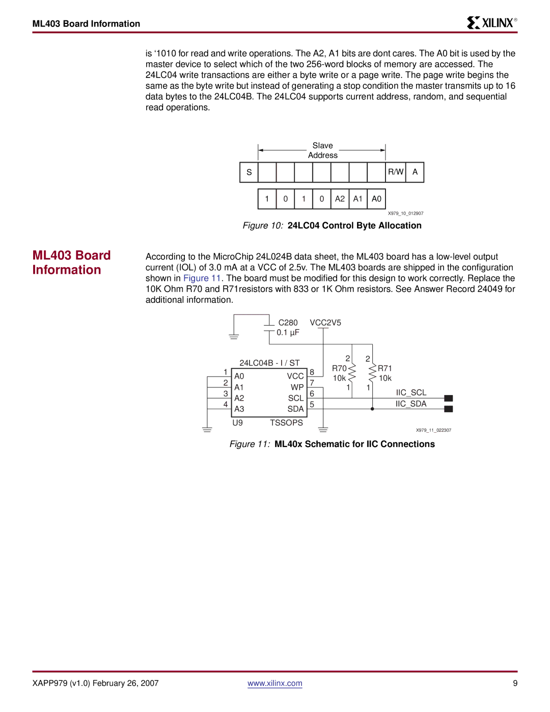
Figure 10: 24LC04 Control Byte Allocation
According to the MicroChip 24L024B data sheet, the ML403 board has a
C280 VCC2V5
0.1 µF
1 | 24LC04B - I / ST | |
A0 | VCC | |
2 | A1 | WP |
3 | A2 | SCL |
4 | A3 | SDA |
|
|
|
| U9 | TSSOPS |
| 2 | 2 |
| |
8 | R70 |
| R71 | |
10k |
| 10k | ||
7 |
| |||
1 | 1 |
| ||
6 | IIC_SCL | |||
|
| |||
5 |
|
| IIC_SDA |
X979_11_022307
Figure 11: ML40x Schematic for IIC Connections
XAPP979 (v1.0) February 26, 2007 | www.xilinx.com | 9 |
