Service Guide
Date Chapter Updates
Revision History
Copyright
Disclaimer
Conventions
Screen messages
Preface
Page
Table of Contents
FRU Field Replaceable Unit List 108
Appendix C Online Support Information 126
123
Microsoft Windows XP Environment Test
Table of Contents
System Specifications
Overview
Features
Performance
Multimedia
Connectivity
Front Panel for Veriton 3600GT/3600V
Label Icon Description
Power LED
Rear Panel for Veriton 3600GT/3600V
Label Icon Color Description
Label Icon Color Description
Front Panel for Veriton 5600GT/5600V
Label Icon Description Optical drive Stop/Eject Button
Rear Panel for Veriton 5600GT/5600V
Label Icon Color Description
Front Panel for Veriton 7600GTR/7600GT/7600V
Optical drive Stop/Eject Button
Rear Panel for Veriton 7600GTR/7600GT/7600V
Label Icon Color Description
Block Diagram
System Block Diagram
Keyboard
Cursor keys
Hardware Specifications and Configurations
Specification
Processor
System Memory
Cache Memory
Video Interface
Audio Interface
IDE Interface
Serial Port
Floppy disk drive Interface
Parallel Port
Switching Power Supply Input frequency
USB Port
Main Board Major Chips
Environmental Requirements
200W Power Supply
250W Power Supply
Input voltage
Input current
Dual Channel Mode
Memory Channel Mode
Single Channel Mode
Memory Characteristics
Total
Maximizing Performance
Ch a
Ch B Ch a
Ch B
System Utilities
Entering Setup
Product Information
Parameter Description
Standard Cmos Features
Parameter Description Options
All, But Keyboard
44 MB, 3.5-inch
None
Press Enter
Auto
LBA
CHS
Enabled
Advanced Bios Features
Disabled
Setup
Fast
Non-OS2
OS2
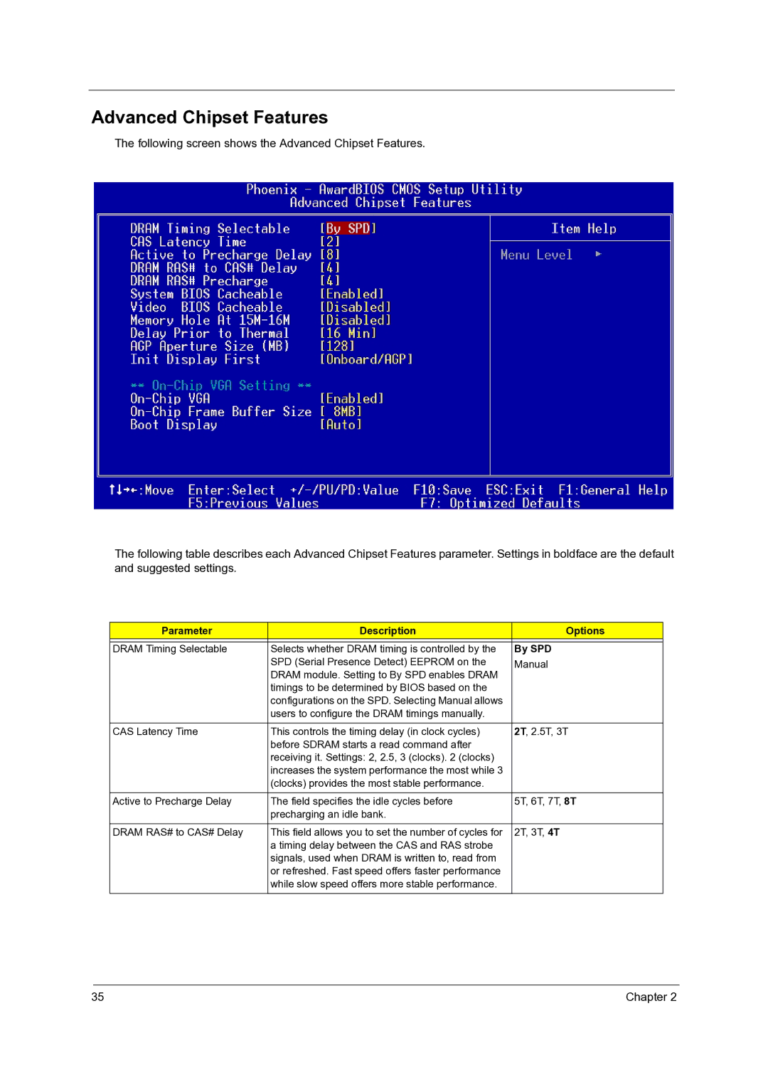
Advanced Chipset Features
By SPD
Onboard/AGP
Integrated Peripherals
OnChip IDE Device
Native Mode
Onboard Device
IDE, RAID
SATA0 Master
SuperIO Device
Button ONLY, Any KEY
Power Management Setup
S1/POS
User Define
Yes
Stop Grant
PCI PIRQA-D #
Delay 4 sec
FAN Control
PnP/PCI Configurations
Auto Escd
Chapter
PC Health Status
Frequency Control
Parameter Description Option
Load Optimized Settings
Set Supervisor Password
System Security
RTC Battery
Set User Password
Bypassing the Password
Cmos Check
Clear Cmos
JBAT1 Clear Cmos
Save & Exit Setup
Exit Without Saving
ATA Operate Mode
Legacy Mode
Intel Serial ATA RAID Introduction
Introduction
Page
Native Mode
Creating, Deleting and Resetting RAID Volumes
RAID Bios Configuration
Using the Intel RAID Option ROM
Create RAID Volume
Page
Chapter
Delete RAID Volume
Reset Disks to Non-RAID
RAID
RAID
Machine Disassembly and Replacement
General Information
Before You Begin
Disassembly Procedure Flowchart
Veriton 7600GTR/GT/V
Veriton 5600GT/V
Veriton 3600GT/V
Opening the Housing
Removing the Housing
Disassembling the Veriton 7600GTR/GT/V
Removing the Front Panel
Chapter
Removing the Internal Cables/Connectors and Memory
Removing the CPU Fan Sink, CPU and System Fan
Removing the Power Supply and Main Board
Removing the Upper Cover and Daughter Board Module
Chapter
Removing the Intrusion Alarm and LCD Module
Disassembling the Veriton 5600GT/V
Page
Removing the CPU Fan Sink and CPU
Removing the System Fan, Power Supply and Main Board
Removing the LED Module and Daughter Board Module
Page
Disassembling the Veriton 3600GT/V
Removing the FDD/ODD/HDD
Page
Removing the Internal Cables/Connectors and Memory
Removing the Internal Cables/Connectors
Removing the System Fan and Main Board
Page
Removing the Upper Case and Power supply
Chapter
Troubleshooting
Power-On Self-Test Post
Checkpoint Description
Reset keyboard for Winbond 977 series Super I/Q chips
Checkpoint Description
Chapter
Auto
Chapter
Hard Disk Install Failure
Post Error Messages List
Bios Messages Action/FRU
Chapter
Error Symptoms List
Error Symptom Action/FRU Processor / Processor Fan
Main board and Memory
Diskette Drive
Error Symptom Action/FRU
Hard Disk Drive
CD/DVD-ROM Drive
Real-Time Clock
Audio
Error Symptom Action/FRU Parallel/Serial Ports
Power Supply
Other Problems
Keyboard
Undetermined Problems
Dimm
Jumper and Connector Information
Jumpers and Connectors
Jumper and Connector Description
Jumper Setting
Label Component
Jumper
Main Board Layout
107 Chapter
FRU Field Replaceable Unit List
Veriton 7600GTR/7600GT/7600V Exploded Diagram
Veriton 5600GT/5600V Exploded Diagram
Veriton 3600GT/3600V Exploded Diagram
Picture Part Name Part Number
HDD 80GB 7200RPM Sata Seagate Alpine ST380013AS
HDD 120G 7200RPM Sata Seagate Alpine ST3120026AS
HDD 160G 7200RPM Sata Seagate Alpine ST3160023AS
HDD 40GB 7200RPM Seagate Cuda VI Alpine ST340014A
For VT7600
Picture Part Name Part Number For VT3600
For VT5600
Corded Mouse USB Optical Genius Powerscroll
VGA Card Radeon 9200 64MB DDR LP W/TV-OUT Ntsc
Leadtek LR2967 VGA Card XABRE200 AGP 8X 32M LP Bracket
Modem Card 56K Askey 1456VQH76DINT
USB KBGRAY, KU0355, US VER., 104KEYS
USB KBGRAY, KU0355, T.CHINESE VER., 104KEYS
USB KBGRAY, KU0355, Intl US VER., 104 Keys
USB KB GRAY, KU0355, Arabic VER., 104 Keys
Wireless KB GRAY, WUR0355, US VER., 104 Keys W/I
MOUSE, Receiver Wireless KB GRAY, WUR0355, T. Chinese VER
MOUSE, Receiver Wireless KB GRAY, WUR0355, Germany VER
MOUSE, Receiver Wireless KB GRAY, WUR0355, Portugese VER
Left Cover
Front Bezel W/ ODD DOOR, FDD COVER, FDD Button
ODD Door W Button
FDD Button
Intrusion Alarm Screw
Internal Speaker 38MM Neosonic
Speaker 5W+5W Active 12V Philips A201S
System FAN W AIR Duck TBD Heatsink W Latch
Chapter 120
Veriton 7600GTR/7600GT/7600V, 5600GT/5600V, 3600GT/3600V
Project Name Trumpet Description
Test Compatible Components
Microsoft Windows XP Environment Test
Appendix B 124
FSP 200W PFC
Appendix B
Online Support Information
127

