Preliminary Information
AMD Athlon™ XP Processor Model 10 Data Sheet | 26237C— May 2003 |
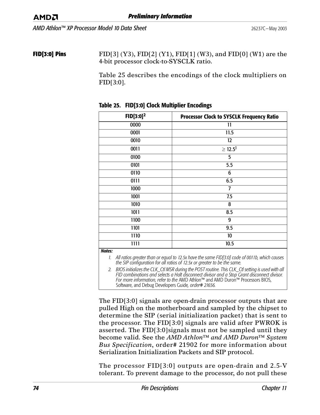
FID[3:0] Pins | FID[3] (Y3), FID[2] (Y1), FID[1] (W3), and FID[0] (W1) are the |
| |
| Table 25 describes the encodings of the clock multipliers on |
| FID[3:0]. |
Table 25. FID[3:0] Clock Multiplier Encodings
FID[3:0]2 | Processor Clock to SYSCLK Frequency Ratio |
0000 | 11 |
|
|
0001 | 11.5 |
|
|
0010 | 12 |
|
|
0011 | ≥ 12.51 |
0100 | 5 |
|
|
0101 | 5.5 |
|
|
0110 | 6 |
|
|
0111 | 6.5 |
|
|
1000 | 7 |
|
|
1001 | 7.5 |
|
|
1010 | 8 |
|
|
1011 | 8.5 |
|
|
1100 | 9 |
|
|
1101 | 9.5 |
|
|
1110 | 10 |
|
|
1111 | 10.5 |
|
|
Notes:
1. All ratios greater than or equal to 12.5x have the same FID[3:0] code of 0011b, which causes the SIP configuration for all ratios of 12.5x or greater to be the same.
2. BIOS initializes the CLK_Ctl MSR during the POST routine. This CLK_Ctl setting is used with all FID combinations and selects a Halt disconnect divisor and a Stop Grant disconnect divisor. For more information, refer to the AMD Athlon™ and AMD Duron™ Processors BIOS, Software, and Debug Developers Guide, order# 21656.
The FID[3:0] signals are
The processor FID[3:0] outputs are
74 | Pin Descriptions | Chapter 11 |