Manuals
/
Analog Devices
/
TV and Video
/
TV Converter Box
Analog Devices
HSC-ADC-EVALC
warranty
Rev Page 18
Models:
HSC-ADC-EVALC
1
18
32
32
Download
32 pages
49.14 Kb
15
16
17
18
19
20
21
22
Functional Block Diagram
Configuration Eeprom
Connection and Setup
Connector J2
U4 DIP Switch Setting
Sram and Fpga Power
Page 18
Image 18
HSC-ADC-EVALC
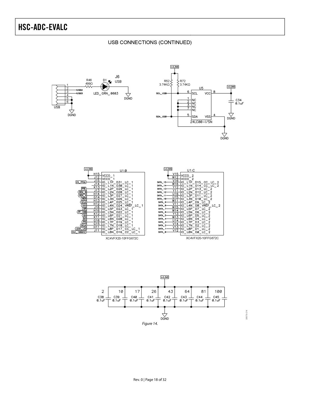
USB CONNECTIONS (CONTINUED)
J6
R46
R52
R72
499Ω
1
3.74KΩ
3.74KΩ
2
3
4
5
6
XC4VFX20-10FFG672C
XC4VFX20-10FFG672C
06676-014
Figure 14.
Rev. 0 Page 18 of 32
Page 17
Page 19
Page 18
Image 18
Page 17
Page 19
Contents
Equipment Needed
Features
Functional Block Diagram
Product Highlights
HSC-ADC-EVALC Table of Contents
HSC-ADC-EVALC
Product Description
Evaluation Board Description
Power Supplies
Connection and Setup
HSC-ADC-EVALC ADC Capture Board Easy Start
U4 DIP Switch Setting
Jumpers
Jumper Number Description
HSC-ADC-EVALC ADC Capture Board Features
HSC-ADC-EVALC Components Top View
HSC-ADC-EVALC Supported ADC Evaluation Boards
HSC-ADC-EVALC Components Bottom View
HSC-ADC-EVALC Theory of Operation
HSC-ADC-EVALC Evaluation Board Schematics and Artwork
HSC-ADC-EVALC Schematics
Sram Address and Control
Fpga to Sram Data
AD19 to be Used with Higher Density Sram Devices
Sram and Fpga Power
Sram a Bypass CAP
Unused Rocket I/0 Connections
Rocket I/0 Connections
USB Connections
Rev Page 18
EZ-KIT Expansion Interface for DSPs
Tyco HM
Configuration Eeprom
Power and Voltage Regulators
PCB Layout
Top Silkscreen
HSC-ADC-EVALC
J1 HS-SERIAL/SPI/AUX
Connector J2
Schematic Net Name Fpga Pin
Connector J3
HSC-ADC-EVALC J3 I/O Connections to Fpga U1
Manufacturer
HSC-ADC-EVALC Ordering Information
Qty
Part Number
Qty Reference Designator Description
R16
Ordering Guide ESD Caution
Model Description
Rev Page 31
Rev Page 32
Top
Page
Image
Contents