PRELIMINARY | CY14B104K, CY14B104M |
|
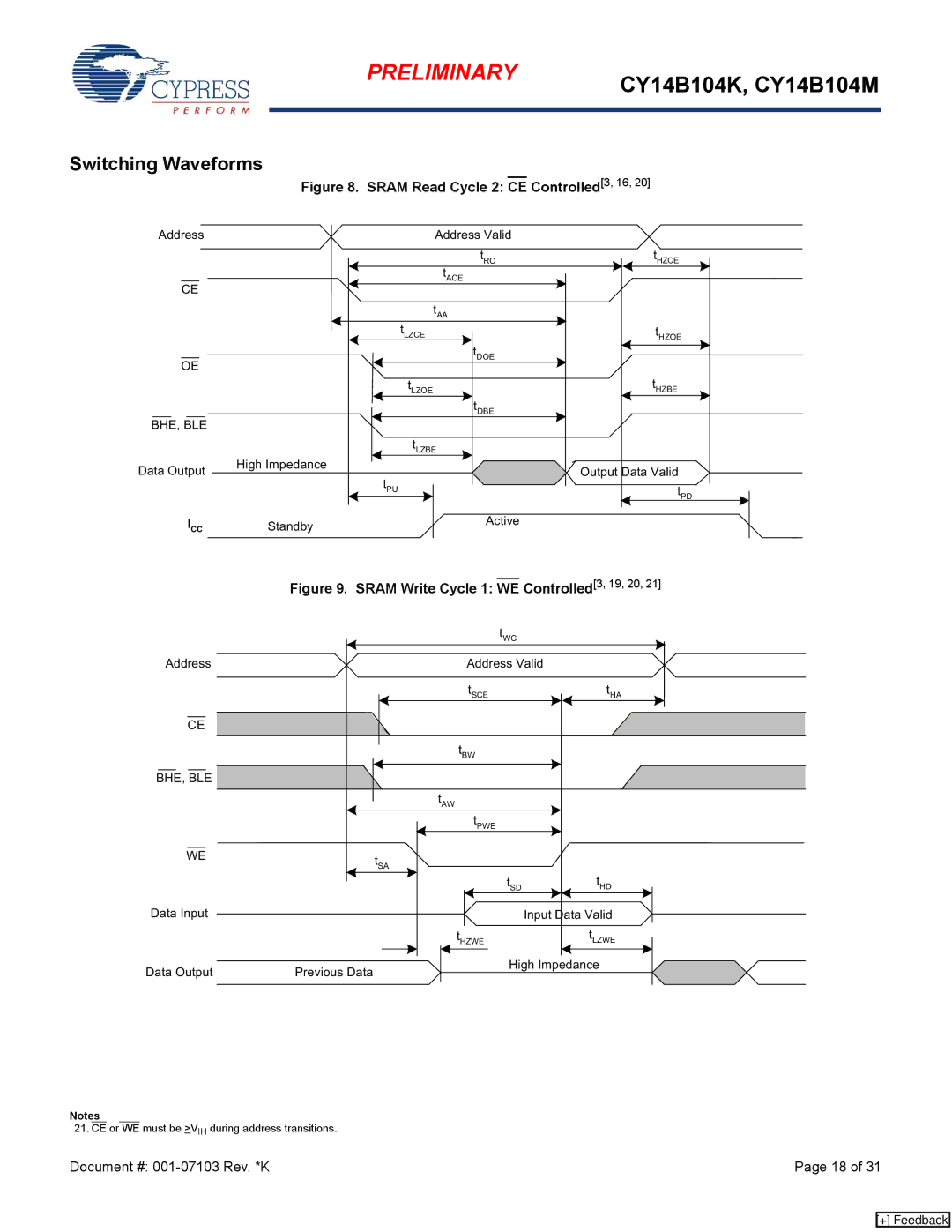
Switching Waveforms
Figure 8. SRAM Read Cycle 2: CE Controlled[3, 16, 20]
Address | Address Valid |
|
| tRC | tHZCE |
CE |
| tACE |
|
|
|
| |
|
| tAA |
|
|
| tLZCE | t |
|
|
| HZOE |
OE |
| tDOE |
|
|
|
| |
|
| tLZOE | tHZBE |
|
| tDBE |
|
BHE, BLE |
|
|
|
|
| tLZBE |
|
Data Output | High Impedance |
| Output Data Valid |
| tPU | ||
|
| tPD | |
|
|
| |
ICC | Standby | Active |
|
| Figure 9. SRAM Write Cycle 1: WE Controlled[3, 19, 20, 21] | ||
|
| tWC |
|
Address |
| Address Valid | |
|
| tSCE | tHA |
CE |
|
|
|
|
| tBW |
|
BHE, BLE |
|
|
|
|
| tAW |
|
|
| tPWE |
|
WE |
| tSA |
|
|
|
| |
|
| tSD | tHD |
Data Input |
|
| Input Data Valid |
|
| tHZWE | tLZWE |
Data Output | Previous Data | High Impedance | |
|
| ||
Notes
21. CE or WE must be >VIH during address transitions.
Document #: | Page 18 of 31 |
[+] Feedback