|
|
|
|
|
| PRELIMINARY | CY14B104K, CY14B104M | ||
|
|
|
|
|
|
|
|
| |
|
|
|
|
|
|
|
|
|
|
|
|
|
|
|
|
|
|
| |
Table 1. Pin Definitions (continued) |
| ||||||||
|
|
|
|
|
|
|
| ||
Pin Name | I/O Type |
|
|
|
| Description |
| ||
| INT | Output | Interrupt Output. Programmable to respond to the clock alarm, the watchdog timer, and the power | ||||||
|
| monitor. Also programmable to either active HIGH (push or pull) or LOW (open drain). | |||||||
|
|
|
| ||||||
| VSS | Ground | Ground for the Device. Must be connected to ground of the system. | ||||||
| VCC | Power Supply | Power Supply Inputs to the Device. 3.0V +20%, |
| |||||
|
|
| Input/Output | Hardware STORE Busy | (HSB) | . When LOW this output indicates that a Hardware STORE is in progress. | |||
| HSB |
|
| When pulled LOW external to the chip it initiates a nonvolatile STORE operation. A weak internal pull | |||||
|
|
|
| up resistor keeps this pin HIGH if not connected (connection optional). After each STORE operation | |||||
|
|
|
| HSB is driven HIGH for short time with standard output high current. | |||||
VCAP | Power Supply | AutoStore Capacitor. Supplies power to the nvSRAM during power loss to store data from SRAM to | |||||||
|
|
|
| nonvolatile elements. |
| ||||
Device Operation
The CY14B104K/CY14B104M nvSRAM is made up of two functional components paired in the same physical cell. These are a SRAM memory cell and a nonvolatile QuantumTrap cell. The SRAM memory cell operates as a standard fast static RAM. Data in the SRAM is transferred to the nonvolatile cell (the STORE operation), or from the nonvolatile cell to the SRAM (the RECALL operation). Using this unique architecture, all cells are stored and recalled in parallel. During the STORE and RECALL operations SRAM read and write operations are inhibited. The CY14B104K/CY14B104M supports infinite reads and writes similar to a typical SRAM. In addition, it provides infinite RECALL operations from the nonvolatile cells and up to 200K STORE operations. See the “Truth Table For SRAM Operations” on page 23 for a complete description of read and write modes.
SRAM Read
The CY14B104K/CY14B104M performs a read cycle whenever CE and OE are LOW, and WE and HSB are HIGH. The address specified on pins
SRAM Write
A write cycle is performed when CE and WE are LOW and HSB is HIGH. The address inputs must be stable before entering the write cycle and must remain stable until CE or WE goes HIGH at the end of the cycle. The data on the common I/O pins
AutoStore Operation
The CY14B104K/CY14B104M stores data to the nvSRAM using one of three storage operations. These three operations are: Hardware STORE, activated by the HSB; Software STORE, activated by an address sequence; AutoStore, on device power down. The AutoStore operation is a unique feature of QuantumTrap technology and is enabled by default on the CY14B104K/CY14B104M.
During normal operation, the device draws current from VCC to charge a capacitor connected to the VCAP pin. This stored charge is used by the chip to perform a single STORE operation. If the voltage on the VCC pin drops below VSWITCH, the part automatically disconnects the VCAP pin from VCC. A STORE operation is initiated with power provided by the VCAP capacitor.
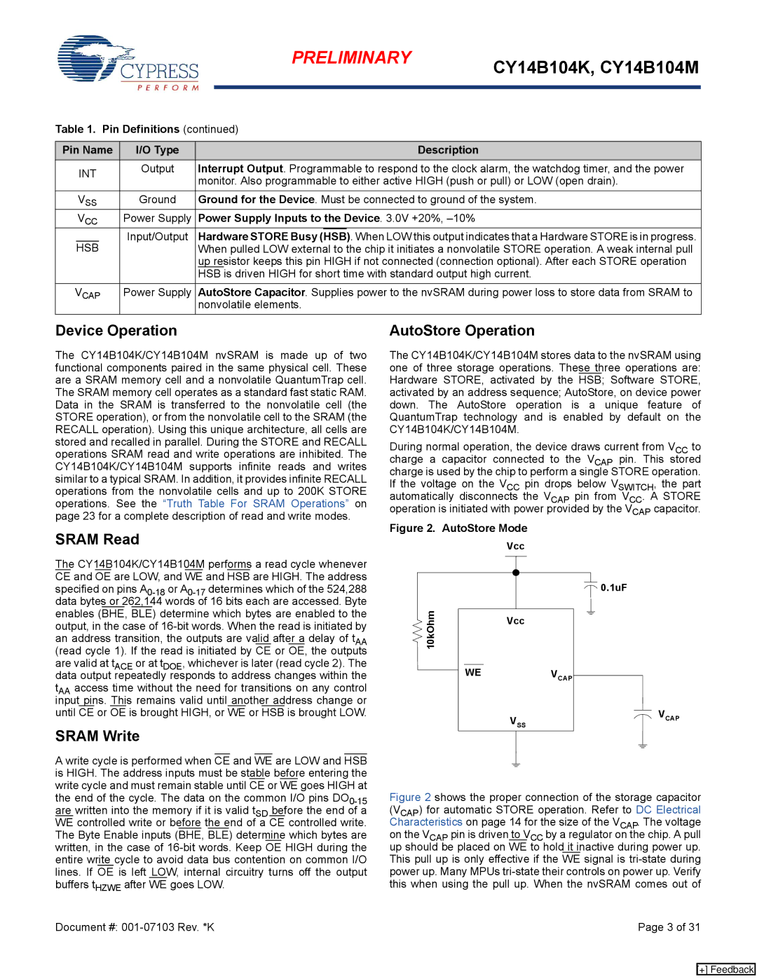
Figure 2. AutoStore Mode
| Vcc | |
10kOhm | 0.1uF | |
Vcc | ||
| ||
WE | VCAP | |
| VCAP | |
| VSS |
Figure 2 shows the proper connection of the storage capacitor (VCAP) for automatic STORE operation. Refer to DC Electrical Characteristics on page 14 for the size of the VCAP. The voltage on the VCAP pin is driven to VCC by a regulator on the chip. A pull up should be placed on WE to hold it inactive during power up. This pull up is only effective if the WE signal is tri-state during power up. Many MPUs tri-state their controls on power up. Verify this when using the pull up. When the nvSRAM comes out of
Document #: | Page 3 of 31 |
[+] Feedback