PRELIMINARY | CY14B104K, CY14B104M |
|
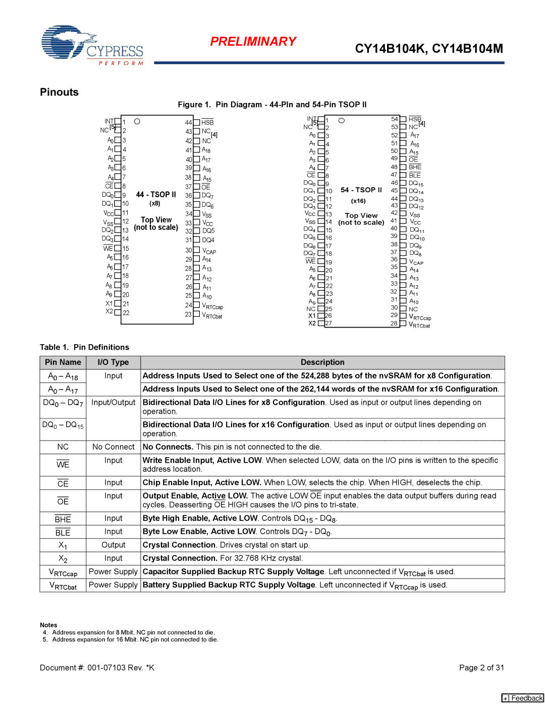
Pinouts
Figure 1. Pin Diagram - 44-PIn and 54-Pin TSOP II
INT
NC[5]
A0 ![]()
A1 ![]()
A2 ![]()
A3 ![]() A4
A4 ![]()
CE ![]()
DQ0 ![]() DQ1
DQ1 ![]()
VCC ![]()
VSS ![]()
DQ2 ![]() DQ3
DQ3 ![]()
WE ![]() A5
A5 ![]() A6
A6 ![]() A7
A7 ![]() A8
A8 ![]() A9
A9 ![]() X1
X1 ![]() X2
X2 ![]()
1 |
|
|
|
|
|
|
|
| INT |
|
| 1 |
| 54 |
|
|
| HSB |
| |||||||
| 44 |
|
| HSB |
| |||||||||||||||||||||
2 |
|
|
| NC[5] |
|
| 2 |
| 53 |
|
|
| NC [4] | |||||||||||||
| 43 |
|
| NC[4] |
| A |
|
| 3 |
| 52 |
|
|
| A | |||||||||||
|
|
|
|
|
|
|
| |||||||||||||||||||
|
|
|
|
|
| |||||||||||||||||||||
3 |
| 42 |
|
| NC | 0 |
|
|
|
|
|
|
|
|
| 17 |
|
| ||||||||
|
|
|
| A1 |
|
| 4 |
| 51 |
|
|
| A | |||||||||||||
4 |
| 41 |
|
| A18 |
| A |
|
|
| 50 |
| 16 |
|
| |||||||||||
|
|
|
|
|
| 5 |
|
|
|
| A | |||||||||||||||
|
|
|
|
| ||||||||||||||||||||||
5 |
| 40 |
|
| A17 | 2 |
|
|
|
|
|
|
| 49 |
|
| 15 |
|
| |||||||
|
|
|
| A3 |
|
| 6 |
|
|
|
| OE |
|
|
| |||||||||||
6 |
| 39 |
|
|
|
| A4 |
|
|
|
| 48 |
|
|
|
|
| |||||||||
|
|
| A |
|
|
| 7 |
|
|
|
| BHE | ||||||||||||||
|
|
|
|
|
|
| ||||||||||||||||||||
|
|
|
| 16 |
|
|
|
|
|
|
|
|
|
|
|
| 47 |
|
|
|
|
|
|
| ||
7 |
| 38 |
|
| A15 |
| CE |
|
| 8 |
|
|
|
|
| BLE | ||||||||||
8 |
| 37 |
|
|
|
|
| DQ0 |
|
| 9 |
| 46 |
|
|
| DQ15 | |||||||||
44 - TSOP II |
|
| OE |
|
| DQ1 |
|
|
|
|
|
| 10 | 54 - TSOP II | 45 |
|
|
| DQ14 | |||||||
9 | 36 |
|
| DQ7 |
|
|
|
|
|
|
| |||||||||||||||
10 | (x8) | 35 |
|
| DQ6 | DQ2 |
|
| 11 | (x16) | 44 |
|
|
| DQ13 | |||||||||||
|
| DQ3 |
|
|
| 12 |
| 43 |
|
|
| DQ12 | ||||||||||||||
11 |
|
|
|
|
|
|
|
|
| |||||||||||||||||
| 34 |
|
| V | VCC |
|
| 13 | Top View | 42 |
|
|
| V | ||||||||||||
12 | Top View |
|
|
| SS | VSS |
|
|
|
|
| 41 |
|
|
| SS | ||||||||||
33 |
|
| VCC |
|
|
|
| 14 | (not to scale) |
|
|
| V | |||||||||||||
| (not to scale) |
|
| DQ |
|
|
|
| 40 |
|
|
| CC | |||||||||||||
13 |
| 32 |
|
| DQ5 | 4 |
|
|
|
|
|
| 15 |
| 39 |
|
|
| DQ11 | |||||||
|
|
|
|
|
|
|
|
|
|
|
|
| ||||||||||||||
14 |
| 31 |
|
| DQ4 | DQ5 |
|
|
|
|
| 16 |
| 38 |
|
|
| DQ10 | ||||||||
|
|
|
|
|
|
|
|
|
| |||||||||||||||||
15 |
| 30 |
|
| VCAP | DQ6 |
|
|
|
|
| 17 |
|
|
|
| DQ9 | |||||||||
16 |
|
|
| DQ7 |
|
|
| 18 |
| 37 |
|
|
| DQ8 | ||||||||||||
| 29 |
|
| A14 |
|
|
|
|
|
|
|
|
|
|
| 36 |
|
|
|
|
|
|
| |||
17 |
| 28 |
|
| A13 |
| WE |
|
|
| 19 |
| 35 |
|
|
| VCAP | |||||||||
|
|
|
| A |
|
|
| 20 |
|
|
|
| A | |||||||||||||
18 |
| 27 |
|
| A12 | 5 |
|
|
|
|
|
|
| 34 |
|
|
| 14 |
|
| ||||||
|
|
|
| A6 |
|
| 21 |
|
|
|
| A13 | ||||||||||||||
19 |
|
|
|
|
|
| 33 |
|
| |||||||||||||||||
| 26 |
|
| A |
| A7 |
|
| 22 |
|
|
|
| A12 | ||||||||||||
|
|
|
|
|
|
|
|
| ||||||||||||||||||
20 |
|
|
| 11 |
|
| A8 |
|
|
|
|
|
| 23 |
| 32 |
|
|
| A11 | ||||||
| 25 |
|
| A10 |
|
|
|
|
|
|
|
| 31 |
|
|
| ||||||||||
21 |
| 24 |
|
| VRTCcap |
| A9 |
|
|
|
| 24 |
| 30 |
|
|
| A10 | ||||||||
|
|
|
|
| ||||||||||||||||||||||
|
|
|
|
|
|
|
|
|
|
| ||||||||||||||||
22 |
|
|
|
| NC |
|
| 25 |
|
|
|
| NC | |||||||||||||
|
|
|
| |||||||||||||||||||||||
| 23 |
|
| VRTCbat |
| X1 |
|
| 26 |
| 29 |
|
|
| V | |||||||||||
|
|
|
| |||||||||||||||||||||||
|
|
|
|
|
|
|
|
| X2 |
| 27 |
| 28 |
|
|
| RTCcap | |||||||||
|
|
|
|
|
|
|
|
|
|
|
|
|
| VRTCbat | ||||||||||||
|
|
|
|
|
|
|
|
| ||||||||||||||||||
|
|
|
|
|
|
|
|
|
|
|
|
| ||||||||||||||
Table 1. Pin Definitions
Pin Name | I/O Type | Description | |||||||||
A0 – A18 | Input | Address Inputs Used to Select one of the 524,288 bytes of the nvSRAM for x8 Configuration. | |||||||||
A0 – A17 |
| Address Inputs Used to Select one of the 262,144 words of the nvSRAM for x16 Configuration. | |||||||||
DQ0 – DQ7 | Input/Output | Bidirectional Data I/O Lines for x8 Configuration. Used as input or output lines depending on | |||||||||
|
|
|
|
|
|
|
|
| operation. | ||
DQ0 – DQ15 |
| Bidirectional Data I/O Lines for x16 Configuration. Used as input or output lines depending on | |||||||||
|
|
|
|
|
|
|
|
| operation. | ||
|
| NC | No Connect | No Connects. This pin is not connected to the die. | |||||||
|
|
|
|
|
|
|
|
|
| ||
|
|
|
|
|
|
|
| Input | Write Enable Input, Active LOW. When selected LOW, data on the I/O pins is written to the specific | ||
|
| WE | |||||||||
|
|
| address location. | ||||||||
|
|
|
|
|
|
|
|
| |||
|
|
|
|
|
|
|
|
| |||
|
|
|
|
|
|
| Input | Chip Enable Input, Active LOW. When LOW, selects the chip. When HIGH, deselects the chip. | |||
|
|
| CE | ||||||||
|
|
|
|
|
|
|
| Input | Output Enable, Active LOW. The active LOW |
| input enables the data output buffers during read |
|
|
|
|
|
|
|
| OE | |||
|
| OE | |||||||||
|
|
| cycles. Deasserting OE HIGH causes the I/O pins to | ||||||||
|
|
|
|
|
|
|
|
| |||
|
|
|
|
|
| ||||||
|
|
|
|
|
|
|
| Input | Byte High Enable, Active LOW. Controls DQ15 - DQ8. | ||
| BHE | ||||||||||
|
|
|
|
|
|
| Input | Byte Low Enable, Active LOW. Controls DQ7 - DQ0. | |||
| BLE | ||||||||||
|
|
| X1 | Output | Crystal Connection. Drives crystal on start up. | ||||||
|
|
| X2 | Input | Crystal Connection. For 32.768 KHz crystal. | ||||||
VRTCcap | Power Supply | Capacitor Supplied Backup RTC Supply Voltage. Left unconnected if VRTCbat is used. | |||||||||
VRTCbat | Power Supply | Battery Supplied Backup RTC Supply Voltage. Left unconnected if VRTCcap is used. | |||||||||
Notes
4.Address expansion for 8 Mbit. NC pin not connected to die.
5.Address expansion for 16 Mbit. NC pin not connected to die.
Document #: | Page 2 of 31 |
[+] Feedback