CY7C1360C
CY7C1362C
conducted, the data presented to the DQs is written into the corresponding address location in the memory core. If a Byte Write is conducted, only the selected bytes are written. Bytes not selected during a Byte Write operation will remain unaltered. A synchronous
Because the CY7C1360C/CY7C1362C is a common I/O device, the Output Enable (OE) must be deasserted HIGH before presenting data to the DQs inputs. Doing so will
Burst Sequences
The CY7C1360C/CY7C1362C provides a
Asserting ADV LOW at clock rise will automatically increment the burst counter to the next address in the burst sequence. Both Read and Write burst operations are supported.
Sleep Mode
The ZZ input pin is an asynchronous input. Asserting ZZ places the SRAM in a power conservation “sleep” mode. Two
clock cycles are required to enter into or exit from this “sleep” mode. While in this mode, data integrity is guaranteed. Accesses pending when entering the “sleep” mode are not considered valid nor is the completion of the operation guaranteed. The device must be deselected prior to entering the “sleep” mode. CE1, CE2, CE3[2], ADSP, and ADSC must remain inactive for the duration of tZZREC after the ZZ input returns LOW.
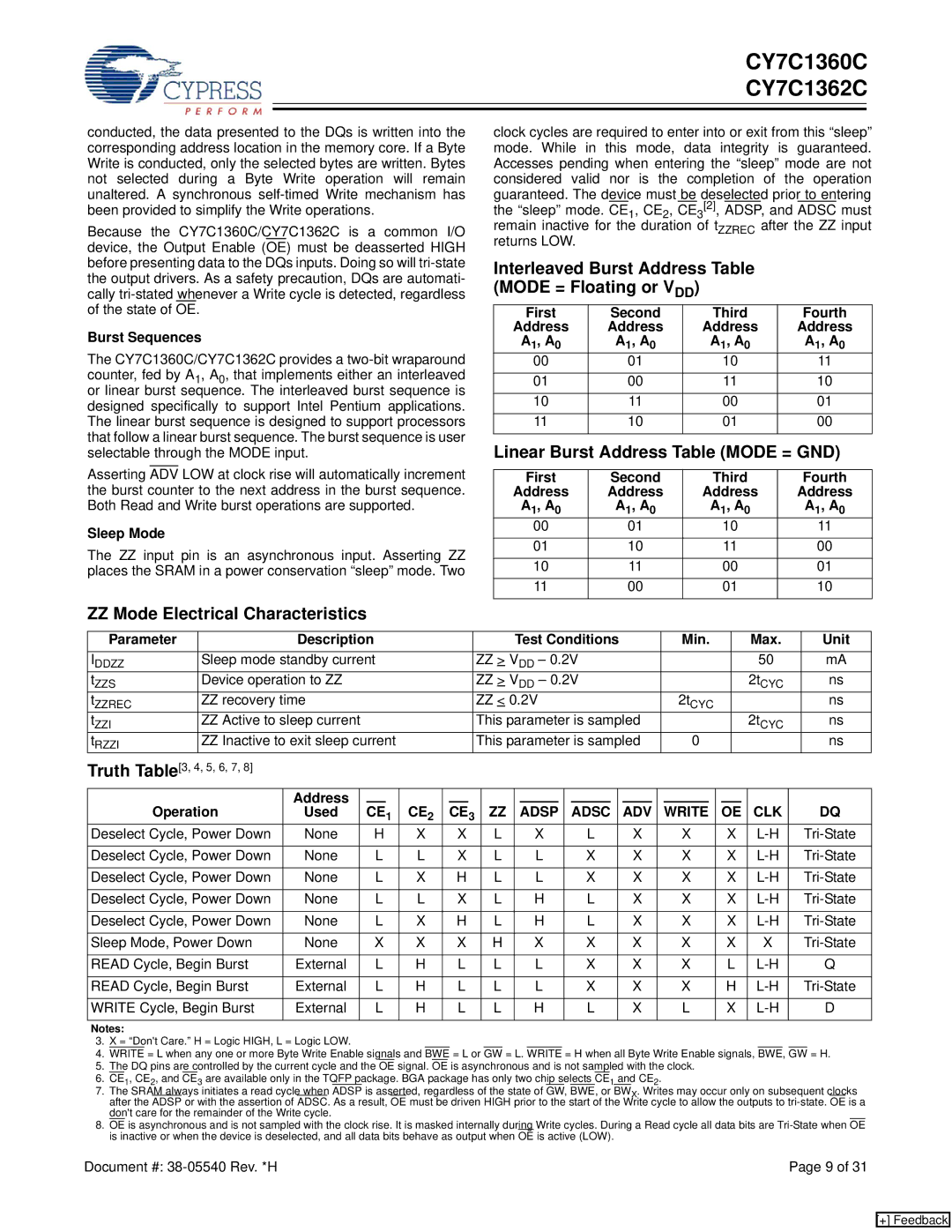
Interleaved Burst Address Table (MODE = Floating or VDD)
First | Second | Third | Fourth |
Address | Address | Address | Address |
A1, A0 | A1, A0 | A1, A0 | A1, A0 |
00 | 01 | 10 | 11 |
01 | 00 | 11 | 10 |
10 | 11 | 00 | 01 |
11 | 10 | 01 | 00 |
Linear Burst Address Table (MODE = GND)
First | Second | Third | Fourth |
Address | Address | Address | Address |
A1, A0 | A1, A0 | A1, A0 | A1, A0 |
00 | 01 | 10 | 11 |
01 | 10 | 11 | 00 |
10 | 11 | 00 | 01 |
11 | 00 | 01 | 10 |
ZZ Mode Electrical Characteristics
Parameter |
| Description |
|
|
|
|
|
|
| Test Conditions |
|
|
|
| Min. |
|
|
| Max. | Unit | |||||||||||||
IDDZZ |
| Sleep mode standby current |
|
|
|
|
| ZZ > VDD – 0.2V |
|
|
|
|
|
|
|
|
| 50 |
| mA | |||||||||||||
tZZS |
| Device operation to ZZ |
|
|
|
|
|
|
| ZZ > VDD – 0.2V |
|
|
|
|
|
|
|
|
|
| 2tCYC | ns | |||||||||||
tZZREC |
| ZZ recovery time |
|
|
|
|
|
|
| ZZ < 0.2V |
|
|
|
|
|
|
| 2tCYC |
|
|
|
|
| ns | |||||||||
tZZI |
| ZZ Active to sleep current |
|
|
|
|
|
|
| This parameter is sampled |
|
|
|
|
|
|
|
|
| 2tCYC | ns | ||||||||||||
tRZZI |
| ZZ Inactive to exit sleep current |
|
|
|
|
| This parameter is sampled |
|
| 0 |
|
|
|
|
|
|
| ns | ||||||||||||||
Truth Table[3, 4, 5, 6, 7, 8] |
|
|
|
|
|
|
|
|
|
|
|
|
|
|
|
|
|
|
|
|
|
|
|
|
|
|
|
|
|
|
| ||
|
|
| Address |
|
|
|
|
|
|
|
|
|
|
|
|
|
|
|
|
|
|
|
|
|
|
|
|
|
|
|
|
|
|
| Operation | Used |
| CE | 1 | CE2 |
| CE | 3 |
| ZZ |
| ADSP |
|
| ADSC |
|
| ADV |
|
|
| WRITE |
|
| OE |
| CLK |
| DQ | |||
Deselect Cycle, Power Down | None |
| H | X |
| X |
| L |
| X |
| L |
| X |
|
|
| X |
| X |
|
| |||||||||||
|
|
|
|
|
|
|
|
|
|
|
|
|
|
|
|
|
|
|
|
|
|
|
|
| |||||||||
Deselect Cycle, Power Down | None |
| L | L |
| X |
| L |
| L |
| X |
| X |
|
|
| X |
| X |
|
| |||||||||||
|
|
|
|
|
|
|
|
|
|
|
|
|
|
|
|
|
|
|
|
|
|
|
|
| |||||||||
Deselect Cycle, Power Down | None |
| L | X |
| H |
| L |
| L |
| X |
| X |
|
|
| X |
| X |
|
| |||||||||||
|
|
|
|
|
|
|
|
|
|
|
|
|
|
|
|
|
|
|
|
|
|
|
|
| |||||||||
Deselect Cycle, Power Down | None |
| L | L |
| X |
| L |
| H |
| L |
| X |
|
|
| X |
| X |
|
| |||||||||||
|
|
|
|
|
|
|
|
|
|
|
|
|
|
|
|
|
|
|
|
|
|
|
|
| |||||||||
Deselect Cycle, Power Down | None |
| L | X |
| H |
| L |
| H |
| L |
| X |
|
|
| X |
| X |
|
| |||||||||||
|
|
|
|
|
|
|
|
|
|
|
|
|
|
|
|
|
|
|
|
|
|
|
|
| |||||||||
Sleep Mode, Power Down | None |
| X | X |
| X |
| H |
| X |
| X |
| X |
|
|
| X |
| X |
| X |
| ||||||||||
|
|
|
|
|
|
|
|
|
|
|
|
|
|
|
|
|
|
|
|
|
|
|
|
| |||||||||
READ Cycle, Begin Burst | External |
| L | H |
| L |
| L |
| L |
| X |
| X |
|
|
| X |
| L |
|
| Q | ||||||||||
|
|
|
|
|
|
|
|
|
|
|
|
|
|
|
|
|
|
|
|
|
|
|
|
| |||||||||
READ Cycle, Begin Burst | External |
| L | H |
| L |
| L |
| L |
| X |
| X |
|
|
| X |
| H |
|
| |||||||||||
|
|
|
|
|
|
|
|
|
|
|
|
|
|
|
|
|
|
|
|
|
|
|
|
| |||||||||
WRITE Cycle, Begin Burst | External |
| L | H |
| L |
| L |
| H |
| L |
| X |
|
|
| L |
| X |
|
| D | ||||||||||
|
|
|
|
|
|
|
|
|
|
|
|
|
|
|
|
|
|
|
|
|
|
|
|
|
|
|
|
|
|
|
|
|
|
Notes: |
|
|
|
|
|
|
|
|
|
|
|
|
|
|
|
|
|
|
|
|
|
|
|
|
|
|
|
|
|
|
|
|
|
3.X = “Don't Care.” H = Logic HIGH, L = Logic LOW.
4.WRITE = L when any one or more Byte Write Enable signals and BWE = L or GW = L. WRITE = H when all Byte Write Enable signals, BWE, GW = H.
5.The DQ pins are controlled by the current cycle and the OE signal. OE is asynchronous and is not sampled with the clock.
6.CE1, CE2, and CE3 are available only in the TQFP package. BGA package has only two chip selects CE1 and CE2.
7.The SRAM always initiates a read cycle when ADSP is asserted, regardless of the state of GW, BWE, or BWX. Writes may occur only on subsequent clocks after the ADSP or with the assertion of ADSC. As a result, OE must be driven HIGH prior to the start of the Write cycle to allow the outputs to
8.OE is asynchronous and is not sampled with the clock rise. It is masked internally during Write cycles. During a Read cycle all data bits are
Document #: | Page 9 of 31 |
[+] Feedback