CY7C1360C
CY7C1362C
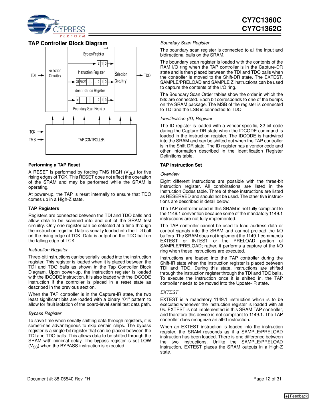
TAP Controller Block Diagram
|
|
|
|
|
|
|
|
|
|
|
|
|
|
|
|
|
|
|
|
|
|
|
|
|
|
|
|
|
|
|
|
|
|
|
|
|
|
|
|
|
| Bypass Register |
|
|
|
|
|
|
| ||||||||
|
|
|
|
|
|
|
|
|
|
|
|
|
|
|
|
|
|
|
|
|
|
|
|
|
|
|
|
|
|
|
|
|
| Selection |
|
|
|
|
|
|
|
|
|
| 2 | 1 |
| 0 |
|
|
|
|
|
| |||
|
|
|
|
|
|
|
|
|
|
|
|
|
|
|
|
|
|
|
|
|
| |||||||
|
|
|
|
|
|
|
|
|
|
|
|
|
|
|
|
|
|
|
|
|
|
|
|
|
| |||
TDI |
|
|
|
|
|
| Instruction Register |
|
|
|
|
| Selection | |||||||||||||||
|
|
| Circuitry |
|
|
|
|
|
|
|
| |||||||||||||||||
|
|
|
|
|
|
|
|
|
|
|
|
|
|
|
|
|
|
|
|
| ||||||||
|
|
|
|
|
|
|
|
|
|
|
|
|
|
|
|
|
|
|
|
|
|
|
|
|
|
| Circuitry | |
|
|
|
|
|
|
|
|
|
|
| 31 | 30 | 29 | . | . | . | 2 | 1 |
| 0 | ||||||||
|
|
|
|
|
|
|
|
|
|
|
|
|
| |||||||||||||||
|
|
|
|
|
|
|
|
|
|
|
|
|
|
|
|
|
|
|
|
|
|
|
|
|
|
|
| |
|
|
|
|
|
|
|
|
|
| Identification Register |
|
|
|
|
|
| ||||||||||||
|
|
|
|
|
|
|
|
|
|
|
|
|
|
|
|
|
|
|
|
|
| |||||||
|
|
|
|
|
|
|
|
|
|
| x | . | . | . | . | . | 2 | 1 |
| 0 |
|
|
|
|
|
| ||
|
|
|
|
|
|
|
|
|
|
|
|
|
|
|
|
|
| |||||||||||
|
|
|
|
|
|
|
|
|
|
|
|
|
|
|
|
|
|
|
|
|
|
|
|
|
|
|
| |
|
|
|
|
|
|
|
|
| Boundary Scan Register |
|
|
|
|
|
| |||||||||||||
TCK |
|
|
|
|
|
|
|
|
|
|
|
|
|
|
|
|
|
|
|
|
|
|
|
|
|
|
|
|
|
|
|
|
|
|
|
|
|
|
|
|
|
|
|
|
|
|
|
|
|
|
|
|
|
|
|
| |
|
|
|
|
|
|
|
|
|
|
|
|
|
|
|
|
|
|
|
|
|
|
|
|
|
|
|
| |
|
|
|
|
|
|
|
|
|
|
|
|
|
|
|
|
|
|
|
|
|
|
|
|
|
| |||
TMS |
|
|
|
|
|
|
|
|
|
| TAP CONTROLLER |
|
|
|
|
|
|
| ||||||||||
|
|
|
|
|
|
|
|
|
|
|
|
|
|
| ||||||||||||||
|
|
|
|
|
|
|
|
|
|
|
|
|
|
|
|
|
|
|
|
|
|
|
|
|
|
|
|
|
Boundary Scan Register
The boundary scan register is connected to all the input and bidirectional balls on the SRAM.
The boundary scan register is loaded with the contents of the RAM I/O ring when the TAP controller is in the
![]() TDO the controller is moved to the
TDO the controller is moved to the
The Boundary Scan Order tables show the order in which the bits are connected. Each bit corresponds to one of the bumps on the SRAM package. The MSB of the register is connected to TDI and the LSB is connected to TDO.
Identification (ID) Register
The ID register is loaded with a
Performing a TAP Reset
A RESET is performed by forcing TMS HIGH (VDD) for five rising edges of TCK. This RESET does not affect the operation of the SRAM and may be performed while the SRAM is operating.
At
TAP Registers
Registers are connected between the TDI and TDO balls and allow data to be scanned into and out of the SRAM test circuitry. Only one register can be selected at a time through the instruction register. Data is serially loaded into the TDI ball on the rising edge of TCK. Data is output on the TDO ball on the falling edge of TCK.
Instruction Register
When the TAP controller is in the
Bypass Register
To save time when serially shifting data through registers, it is sometimes advantageous to skip certain chips. The bypass register is a
TAP Instruction Set
Overview
Eight different instructions are possible with the
The TAP controller used in this SRAM is not fully compliant to the 1149.1 convention because some of the mandatory 1149.1 instructions are not fully implemented.
The TAP controller cannot be used to load address data or control signals into the SRAM and cannot preload the I/O buffers. The SRAM does not implement the 1149.1 commands EXTEST or INTEST or the PRELOAD portion of SAMPLE/PRELOAD; rather, it performs a capture of the I/O ring when these instructions are executed.
Instructions are loaded into the TAP controller during the
EXTEST
EXTEST is a mandatory 1149.1 instruction which is to be executed whenever the instruction register is loaded with all 0s. EXTEST is not implemented in this SRAM TAP controller, and therefore this device is not compliant to 1149.1. The TAP controller does recognize an
When an EXTEST instruction is loaded into the instruction register, the SRAM responds as if a SAMPLE/PRELOAD instruction has been loaded. There is one difference between the two instructions. Unlike the SAMPLE/PRELOAD instruction, EXTEST places the SRAM outputs in a
Document #: | Page 12 of 31 |
[+] Feedback