CY7C1360C
CY7C1362C
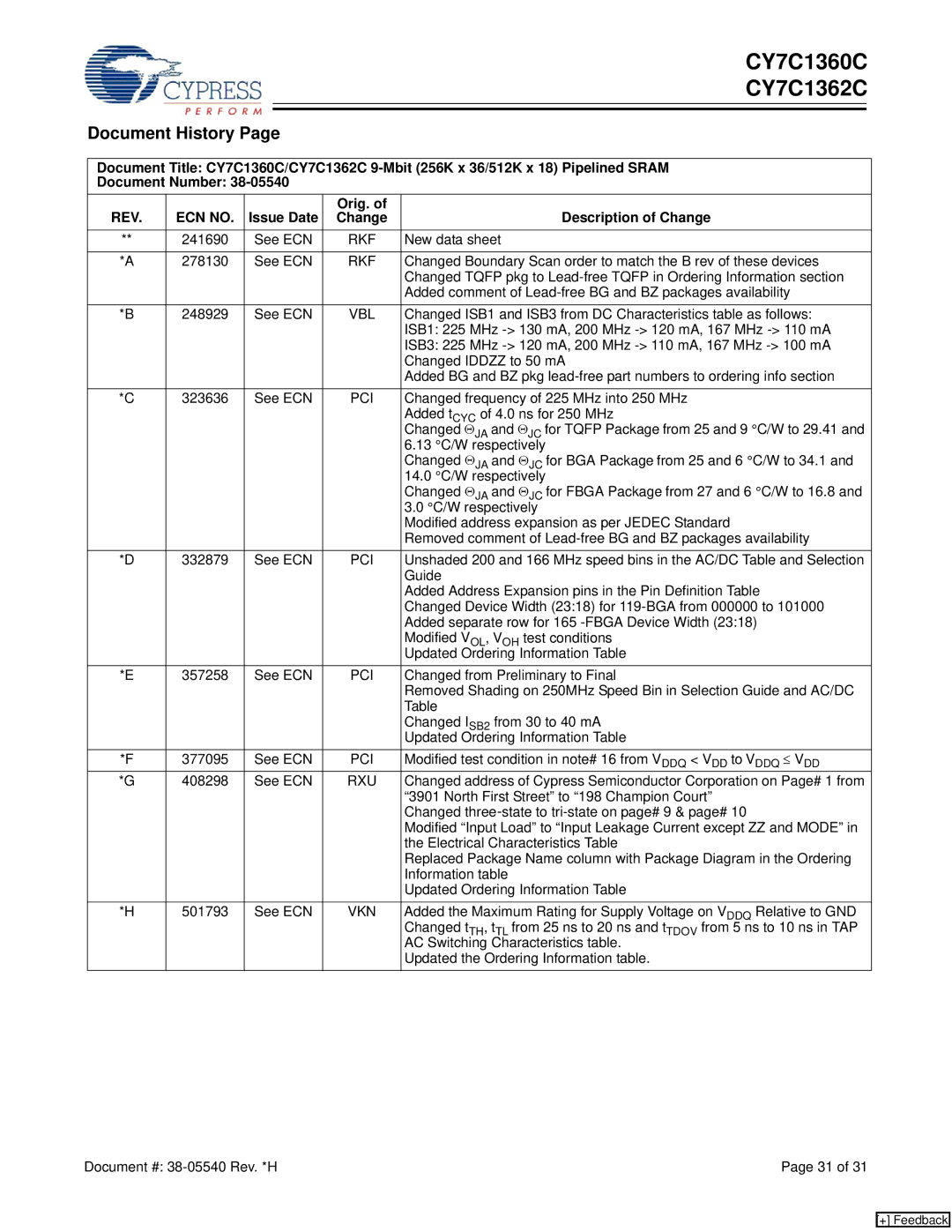
Document History Page
Document Title: CY7C1360C/CY7C1362C
Document Number:
REV. | ECN NO. | Issue Date | Orig. of | Description of Change |
Change | ||||
|
|
|
|
|
** | 241690 | See ECN | RKF | New data sheet |
|
|
|
|
|
*A | 278130 | See ECN | RKF | Changed Boundary Scan order to match the B rev of these devices |
|
|
|
| Changed TQFP pkg to |
|
|
|
| Added comment of |
*B | 248929 | See ECN | VBL | Changed ISB1 and ISB3 from DC Characteristics table as follows: |
|
|
|
| ISB1: 225 MHz |
|
|
|
| ISB3: 225 MHz |
|
|
|
| Changed IDDZZ to 50 mA |
|
|
|
| Added BG and BZ pkg |
*C | 323636 | See ECN | PCI | Changed frequency of 225 MHz into 250 MHz |
|
|
|
| Added tCYC of 4.0 ns for 250 MHz |
|
|
|
| Changed ΘJA and ΘJC for TQFP Package from 25 and 9 °C/W to 29.41 and |
|
|
|
| 6.13 °C/W respectively |
|
|
|
| Changed ΘJA and ΘJC for BGA Package from 25 and 6 °C/W to 34.1 and |
|
|
|
| 14.0 °C/W respectively |
|
|
|
| Changed ΘJA and ΘJC for FBGA Package from 27 and 6 °C/W to 16.8 and |
|
|
|
| 3.0 °C/W respectively |
|
|
|
| Modified address expansion as per JEDEC Standard |
|
|
|
| Removed comment of |
*D | 332879 | See ECN | PCI | Unshaded 200 and 166 MHz speed bins in the AC/DC Table and Selection |
|
|
|
| Guide |
|
|
|
| Added Address Expansion pins in the Pin Definition Table |
|
|
|
| Changed Device Width (23:18) for |
|
|
|
| Added separate row for 165 |
|
|
|
| Modified VOL, VOH test conditions |
|
|
|
| Updated Ordering Information Table |
*E | 357258 | See ECN | PCI | Changed from Preliminary to Final |
|
|
|
| Removed Shading on 250MHz Speed Bin in Selection Guide and AC/DC |
|
|
|
| Table |
|
|
|
| Changed ISB2 from 30 to 40 mA |
|
|
|
| Updated Ordering Information Table |
*F | 377095 | See ECN | PCI | Modified test condition in note# 16 from VDDQ < VDD to VDDQ ≤ VDD |
*G | 408298 | See ECN | RXU | Changed address of Cypress Semiconductor Corporation on Page# 1 from |
|
|
|
| “3901 North First Street” to “198 Champion Court” |
|
|
|
| Changed |
|
|
|
| Modified “Input Load” to “Input Leakage Current except ZZ and MODE” in |
|
|
|
| the Electrical Characteristics Table |
|
|
|
| Replaced Package Name column with Package Diagram in the Ordering |
|
|
|
| Information table |
|
|
|
| Updated Ordering Information Table |
*H | 501793 | See ECN | VKN | Added the Maximum Rating for Supply Voltage on VDDQ Relative to GND |
|
|
|
| Changed tTH, tTL from 25 ns to 20 ns and tTDOV from 5 ns to 10 ns in TAP |
|
|
|
| AC Switching Characteristics table. |
|
|
|
| Updated the Ordering Information table. |
Document #: | Page 31 of 31 |
[+] Feedback