CY7C1360C
CY7C1362C
9-Mbit (256K x 36/512K x 18) Pipelined SRAM
Features
•Supports bus operation up to 250 MHz
•Available speed grades are 250, 200, and 166 MHz
•Registered inputs and outputs for pipelined operation
•3.3V core power supply (VDD)
•2.5V/3.3V I/O operation (VDDQ)
•Fast
— 2.8 ns (for
•Provide
•
Pentium® interleaved or linear burst sequences
•Separate processor and controller address strobes
•Synchronous
•Asynchronous output enable
•Single Cycle Chip Deselect
•Available in
•TQFP Available with
•IEEE 1149.1
Functional Description[1]
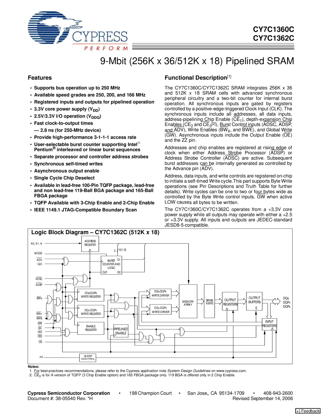
The CY7C1360C/CY7C1362C SRAM integrates 256K x 36 and 512K x 18 SRAM cells with advanced synchronous peripheral circuitry and a
Addresses and chip enables are registered at rising edge of clock when either Address Strobe Processor (ADSP) or Address Strobe Controller (ADSC) are active. Subsequent burst addresses can be internally generated as controlled by the Advance pin (ADV).
Address, data inputs, and write controls are registered
The CY7C1360C/CY7C1362C operates from a +3.3V core power supply while all outputs may operate with either a +2.5 or +3.3V supply. All inputs and outputs are
Logic Block Diagram – CY7C1362C (512K x 18) |
|
|
|
| |||
A0, A1, A | ADDRESS |
|
|
|
|
|
|
REGISTER |
|
|
|
|
|
| |
|
|
|
|
|
|
| |
MODE |
| 2 | A[1:0] |
|
|
|
|
|
|
|
|
|
| ||
|
|
|
|
|
|
| |
ADV |
| BURST | Q1 |
|
|
|
|
CLK | COUNTER AND |
|
|
|
| ||
|
| LOGIC |
|
|
|
|
|
| CLR |
| Q0 |
|
|
|
|
ADSC |
|
|
|
|
|
|
|
ADSP |
|
|
|
|
|
|
|
| DQB,DQPB |
| DQB,DQPB |
|
|
|
|
|
| WRITE DRIVER |
|
|
|
| |
BWB | WRITE REGISTER |
|
|
| OUTPUT | DQs | |
|
|
| OUTPUT | ||||
|
| MEMORY | SENSE | ||||
|
|
| BUFFERS | DQPA | |||
|
|
| AMPS | REGISTERS | |||
|
|
| ARRAY | E | DQPB | ||
| DQA,DQPA |
| DQA,DQPA |
|
| ||
|
|
|
|
| |||
BWA |
| WRITE DRIVER |
|
|
|
| |
WRITE REGISTER |
|
|
|
|
| ||
|
|
|
|
|
| ||
BWE |
|
|
|
|
|
| INPUT |
GW |
|
|
|
|
|
| |
ENABLE |
|
|
|
|
| REGISTERS | |
CE1 | PIPELINED |
|
|
| |||
REGISTER |
|
|
|
| |||
CE2 |
| ENABLE |
|
|
|
| |
CE3 |
|
|
|
|
| ||
|
|
|
|
|
|
| |
OE |
|
|
|
|
|
|
|
ZZ | SLEEP |
|
|
|
|
|
|
CONTROL |
|
|
|
|
|
| |
|
|
|
|
|
|
| |
Notes:
1.For
2.CE3 is for A version of TQFP (3 Chip Enable option) and 165 FBGA package only. 119 BGA is offered only in 2 Chip Enable.
Cypress Semiconductor Corporation | • | 198 Champion Court • San Jose, CA | • | |
Document #: |
| Revised September 14, 2006 | ||
[+] Feedback