CY7C1360C
CY7C1362C
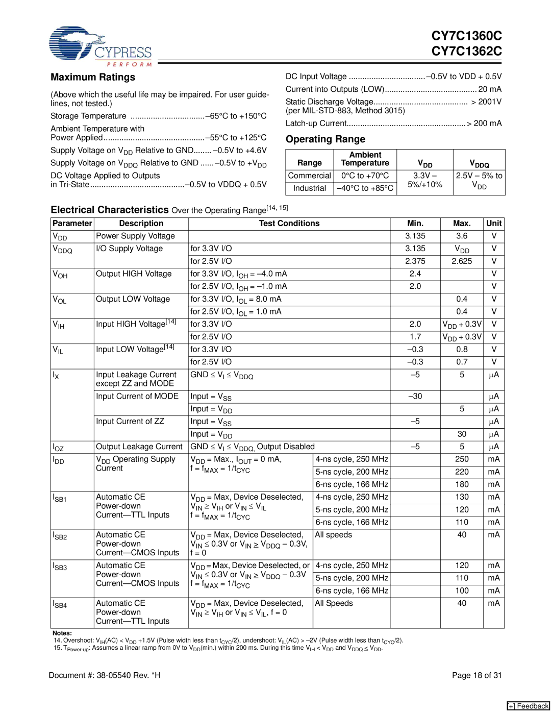
Maximum Ratings
(Above which the useful life may be impaired. For user guide- lines, not tested.)
Storage Temperature | ||
Ambient Temperature with |
|
|
Power Applied | ||
Supply Voltage on VDD Relative to GND | ||
Supply Voltage on VDDQ Relative to GND | ||
DC Voltage Applied to Outputs |
|
|
in | ||
DC Input Voltage | ||||
Current into Outputs (LOW) | 20 mA | |||
Static Discharge Voltage | > 2001V | |||
(per |
|
| ||
> 200 mA | ||||
Operating Range |
|
| ||
|
|
|
|
|
| Ambient |
|
|
|
Range | Temperature |
| VDD | VDDQ |
Commercial | 0°C to +70°C |
| 3.3V – | 2.5V – 5% to |
|
|
| 5%/+10% | VDD |
Industrial |
| |||
Electrical Characteristics Over the Operating Range[14, 15]
Parameter | Description | Test Conditions | Min. | Max. | Unit | ||
VDD | Power Supply Voltage |
|
|
| 3.135 | 3.6 | V |
VDDQ | I/O Supply Voltage | for 3.3V I/O |
| 3.135 | VDD | V | |
|
| for 2.5V I/O |
| 2.375 | 2.625 | V | |
|
|
|
|
|
|
| |
VOH | Output HIGH Voltage | for 3.3V I/O, IOH = |
| 2.4 |
| V | |
|
| for 2.5V I/O, IOH = |
| 2.0 |
| V | |
VOL | Output LOW Voltage | for 3.3V I/O, IOL = 8.0 mA |
|
| 0.4 | V | |
|
| for 2.5V I/O, IOL = 1.0 mA |
|
| 0.4 | V | |
VIH | Input HIGH Voltage[14] | for 3.3V I/O |
| 2.0 | VDD + 0.3V | V | |
|
| for 2.5V I/O |
| 1.7 | VDD + 0.3V | V | |
VIL | Input LOW Voltage[14] | for 3.3V I/O |
| 0.8 | V | ||
|
| for 2.5V I/O |
| 0.7 | V | ||
|
|
|
|
|
|
| |
IX | Input Leakage Current | GND ≤ VI ≤ VDDQ |
| 5 | ∝A | ||
| except ZZ and MODE |
|
|
|
|
|
|
| Input Current of MODE | Input = VSS |
|
| ∝A | ||
|
| Input = VDD |
|
| 5 | ∝A | |
| Input Current of ZZ | Input = VSS |
|
| ∝A | ||
|
| Input = VDD |
|
| 30 | ∝A | |
IOZ | Output Leakage Current | GND ≤ VI ≤ VDDQ, Output Disabled |
| 5 | ∝A | ||
IDD | VDD Operating Supply | VDD = Max., IOUT = 0 mA, |
|
| 250 | mA | |
| Current | f = fMAX = 1/tCYC |
|
|
|
|
|
|
|
| 220 | mA | |||
|
|
|
|
| 180 | mA | |
|
|
|
|
|
|
|
|
ISB1 | Automatic CE | VDD = Max, Device Deselected, |
|
| 130 | mA | |
| VIN ≥ VIH or VIN ≤ VIL |
|
|
|
|
| |
|
|
| 120 | mA | |||
| f = fMAX = 1/tCYC |
|
|
|
|
| |
|
|
| 110 | mA | |||
|
|
|
|
| |||
|
|
|
|
|
|
|
|
ISB2 | Automatic CE | VDD = Max, Device Deselected, |
| All speeds |
| 40 | mA |
| VIN ≤ 0.3V or VIN > VDDQ – 0.3V, |
|
|
|
|
| |
| f = 0 |
|
|
|
|
| |
ISB3 | Automatic CE | VDD = Max, Device Deselected, or |
|
| 120 | mA | |
| VIN ≤ 0.3V or VIN > VDDQ – 0.3V |
|
|
|
|
| |
|
|
| 110 | mA | |||
| f = fMAX = 1/tCYC |
|
|
|
|
| |
|
|
| 100 | mA | |||
|
|
|
|
| |||
|
|
|
|
|
|
|
|
ISB4 | Automatic CE | VDD = Max, Device Deselected, |
| All Speeds |
| 40 | mA |
| VIN ≥ VIH or VIN ≤ VIL, f = 0 |
|
|
|
|
| |
|
|
|
|
|
|
| |
Notes: |
|
|
|
|
|
|
|
14.Overshoot: VIH(AC) < VDD +1.5V (Pulse width less than tCYC/2), undershoot: VIL(AC) >
15.
Document #: | Page 18 of 31 |
[+] Feedback