CY7C1386DV25, CY7C1386FV25
CY7C1387DV25, CY7C1387FV25
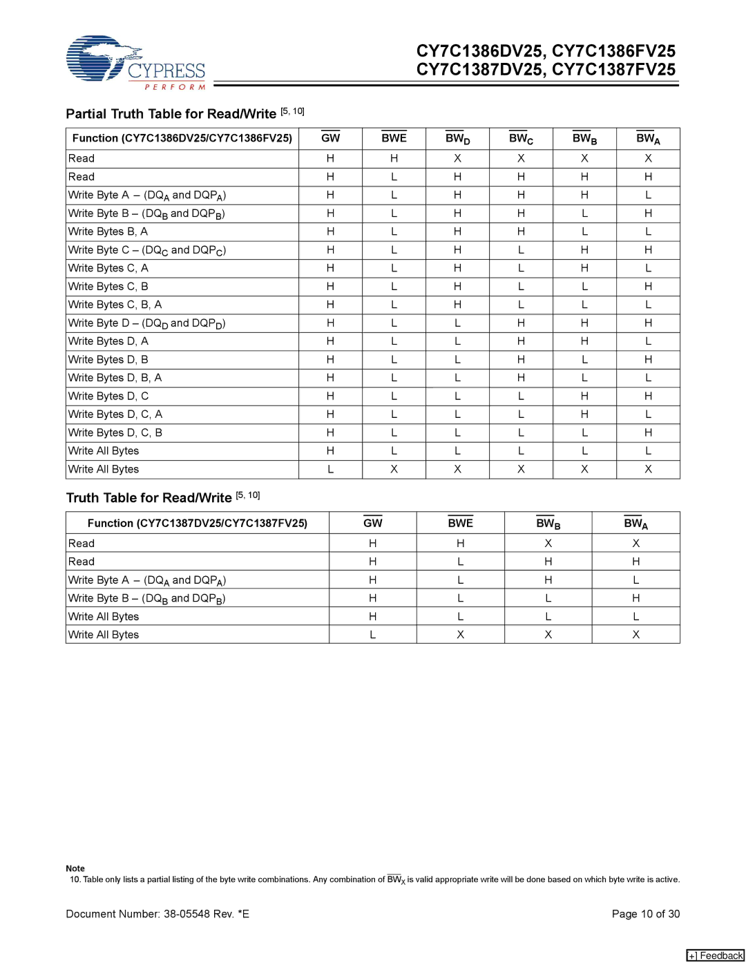
Partial Truth Table for Read/Write [5, 10]
|
|
|
|
|
|
|
|
|
|
|
|
|
|
|
|
|
|
|
Function (CY7C1386DV25/CY7C1386FV25) |
| GW |
|
| BWE |
|
| BWD |
| BWC |
| BWB |
| BWA | ||||
Read |
| H |
|
| H |
|
| X |
| X |
| X |
| X | ||||
|
|
|
|
|
|
|
|
|
|
|
|
|
|
| ||||
Read |
| H |
|
| L |
|
| H |
| H |
| H |
| H | ||||
|
|
|
|
|
|
|
|
|
|
|
|
|
|
| ||||
Write Byte A – (DQA and DQPA) |
| H |
|
| L |
|
| H |
| H |
| H |
| L | ||||
Write Byte B – (DQB and DQPB) |
| H |
|
| L |
|
| H |
| H |
| L |
| H | ||||
Write Bytes B, A |
| H |
|
| L |
|
| H |
| H |
| L |
| L | ||||
|
|
|
|
|
|
|
|
|
|
|
|
|
|
| ||||
Write Byte C – (DQC and DQPC) |
| H |
|
| L |
|
| H |
| L |
| H |
| H | ||||
Write Bytes C, A |
| H |
|
| L |
|
| H |
| L |
| H |
| L | ||||
|
|
|
|
|
|
|
|
|
|
|
|
|
|
| ||||
Write Bytes C, B |
| H |
|
| L |
|
| H |
| L |
| L |
| H | ||||
|
|
|
|
|
|
|
|
|
|
|
|
|
|
| ||||
Write Bytes C, B, A |
| H |
|
| L |
|
| H |
| L |
| L |
| L | ||||
|
|
|
|
|
|
|
|
|
|
|
|
|
|
| ||||
Write Byte D – (DQD and DQPD) |
| H |
|
| L |
|
| L |
| H |
| H |
| H | ||||
Write Bytes D, A |
| H |
|
| L |
|
| L |
| H |
| H |
| L | ||||
|
|
|
|
|
|
|
|
|
|
|
|
|
|
| ||||
Write Bytes D, B |
| H |
|
| L |
|
| L |
| H |
| L |
| H | ||||
|
|
|
|
|
|
|
|
|
|
|
|
|
|
| ||||
Write Bytes D, B, A |
| H |
|
| L |
|
| L |
| H |
| L |
| L | ||||
|
|
|
|
|
|
|
|
|
|
|
|
|
|
| ||||
Write Bytes D, C |
| H |
|
| L |
|
| L |
| L |
| H |
| H | ||||
|
|
|
|
|
|
|
|
|
|
|
|
|
|
| ||||
Write Bytes D, C, A |
| H |
|
| L |
|
| L |
| L |
| H |
| L | ||||
|
|
|
|
|
|
|
|
|
|
|
|
|
|
| ||||
Write Bytes D, C, B |
| H |
|
| L |
|
| L |
| L |
| L |
| H | ||||
|
|
|
|
|
|
|
|
|
|
|
|
|
|
| ||||
Write All Bytes |
| H |
|
| L |
|
| L |
| L |
| L |
| L | ||||
|
|
|
|
|
|
|
|
|
|
|
|
|
|
| ||||
Write All Bytes |
| L |
|
| X |
|
| X |
| X |
| X |
| X | ||||
|
|
|
|
|
|
|
|
|
|
|
|
|
|
|
|
|
|
|
Truth Table for Read/Write [5, 10]
|
|
|
|
|
|
|
|
|
|
|
|
|
Function (CY7C1387DV25/CY7C1387FV25) |
| GW |
|
| BWE |
|
| BWB |
| BWA | ||
Read |
| H |
|
| H |
|
| X |
| X | ||
Read |
| H |
|
| L |
|
| H |
| H | ||
Write Byte A – (DQA and DQPA) |
| H |
|
| L |
|
| H |
| L | ||
Write Byte B – (DQB and DQPB) |
| H |
|
| L |
|
| L |
| H | ||
Write All Bytes |
| H |
|
| L |
|
| L |
| L | ||
Write All Bytes |
| L |
|
| X |
|
| X |
| X | ||
Note
10. Table only lists a partial listing of the byte write combinations. Any combination of BWX is valid appropriate write will be done based on which byte write is active.
Document Number: | Page 10 of 30 |
[+] Feedback