CY7C1386DV25, CY7C1386FV25
CY7C1387DV25, CY7C1387FV25
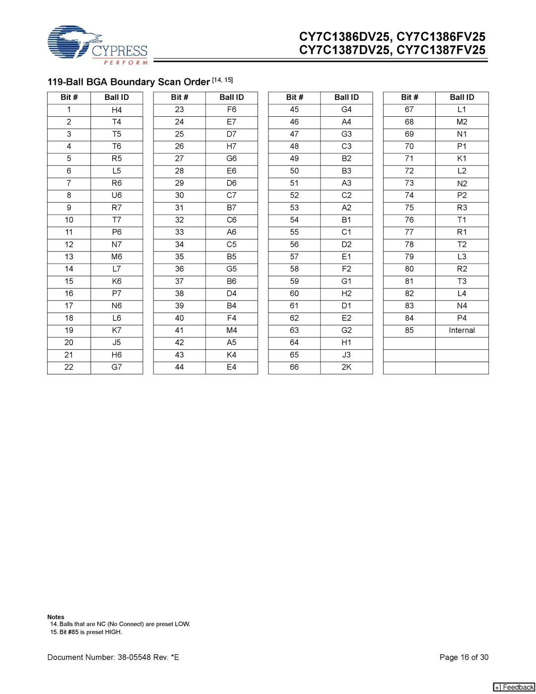
119-Ball BGA Boundary Scan Order [14, 15]
Bit # | Ball ID |
| Bit # | Ball ID |
| Bit # | Ball ID |
| Bit # | Ball ID |
1 | H4 |
| 23 | F6 |
| 45 | G4 |
| 67 | L1 |
|
|
|
|
|
|
|
|
|
|
|
2 | T4 |
| 24 | E7 |
| 46 | A4 |
| 68 | M2 |
|
|
|
|
|
|
|
|
|
|
|
3 | T5 |
| 25 | D7 |
| 47 | G3 |
| 69 | N1 |
|
|
|
|
|
|
|
|
|
|
|
4 | T6 |
| 26 | H7 |
| 48 | C3 |
| 70 | P1 |
|
|
|
|
|
|
|
|
|
|
|
5 | R5 |
| 27 | G6 |
| 49 | B2 |
| 71 | K1 |
|
|
|
|
|
|
|
|
|
|
|
6 | L5 |
| 28 | E6 |
| 50 | B3 |
| 72 | L2 |
|
|
|
|
|
|
|
|
|
|
|
7 | R6 |
| 29 | D6 |
| 51 | A3 |
| 73 | N2 |
|
|
|
|
|
|
|
|
|
|
|
8 | U6 |
| 30 | C7 |
| 52 | C2 |
| 74 | P2 |
|
|
|
|
|
|
|
|
|
|
|
9 | R7 |
| 31 | B7 |
| 53 | A2 |
| 75 | R3 |
|
|
|
|
|
|
|
|
|
|
|
10 | T7 |
| 32 | C6 |
| 54 | B1 |
| 76 | T1 |
|
|
|
|
|
|
|
|
|
|
|
11 | P6 |
| 33 | A6 |
| 55 | C1 |
| 77 | R1 |
|
|
|
|
|
|
|
|
|
|
|
12 | N7 |
| 34 | C5 |
| 56 | D2 |
| 78 | T2 |
|
|
|
|
|
|
|
|
|
|
|
13 | M6 |
| 35 | B5 |
| 57 | E1 |
| 79 | L3 |
|
|
|
|
|
|
|
|
|
|
|
14 | L7 |
| 36 | G5 |
| 58 | F2 |
| 80 | R2 |
|
|
|
|
|
|
|
|
|
|
|
15 | K6 |
| 37 | B6 |
| 59 | G1 |
| 81 | T3 |
|
|
|
|
|
|
|
|
|
|
|
16 | P7 |
| 38 | D4 |
| 60 | H2 |
| 82 | L4 |
|
|
|
|
|
|
|
|
|
|
|
17 | N6 |
| 39 | B4 |
| 61 | D1 |
| 83 | N4 |
|
|
|
|
|
|
|
|
|
|
|
18 | L6 |
| 40 | F4 |
| 62 | E2 |
| 84 | P4 |
|
|
|
|
|
|
|
|
|
|
|
19 | K7 |
| 41 | M4 |
| 63 | G2 |
| 85 | Internal |
|
|
|
|
|
|
|
|
|
|
|
20 | J5 |
| 42 | A5 |
| 64 | H1 |
|
|
|
|
|
|
|
|
|
|
|
|
|
|
21 | H6 |
| 43 | K4 |
| 65 | J3 |
|
|
|
|
|
|
|
|
|
|
|
|
|
|
22 | G7 |
| 44 | E4 |
| 66 | 2K |
|
|
|
|
|
|
|
|
|
|
|
|
|
|
Notes
14.Balls that are NC (No Connect) are preset LOW.
15.Bit #85 is preset HIGH.
Document Number: | Page 16 of 30 |
[+] Feedback