CLK
tCH
tADS tADH
tCL
ADSP
tADS tADH
ADSC
tAS tAH
ADDRESS
GW, BWE,BW
X
CE
ADV
OE
Data Out (DQ)
A1 | A2 | A3 | |
tWES | tWEH | Burst continued with | |
new base address | |||
|
| ||
tCES tCEH |
| Deselect | |
| cycle | ||
|
|
tADVS tADVH
![]() ADV suspends burst
ADV suspends burst
|
| tOEV | tCO |
|
t | tOEHZ | tOELZ | tDOH | tCHZ |
| CLZ |
|
|
|
Q(A1) | Q(A2) | Q(A2 + 1) | Q(A2 + 2) | Q(A2 + 3) | Q(A2) | Q(A2 + 1) | Q(A3) | |
| tCO |
|
|
|
| Burst wraps around |
| |
|
|
|
|
|
|
| ||
| Single READ |
|
| BURST READ |
| to its initial state |
| |
|
|
|
|
|
|
| ||
DON’T CARE
UNDEFINED
Note
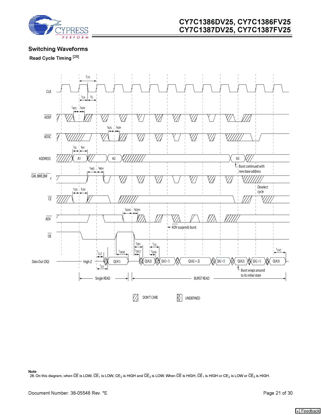
26. On this diagram, when CE is LOW, CE1 is LOW, CE2 is HIGH and CE3 is LOW. When CE is HIGH, CE1 is HIGH or CE2 is LOW or CE3 is HIGH.
Document Number: | Page 21 of 30 |
[+] Feedback