|
|
|
|
|
|
|
|
|
|
|
|
|
|
|
|
| CY7C1386DV25, CY7C1386FV25 | ||||
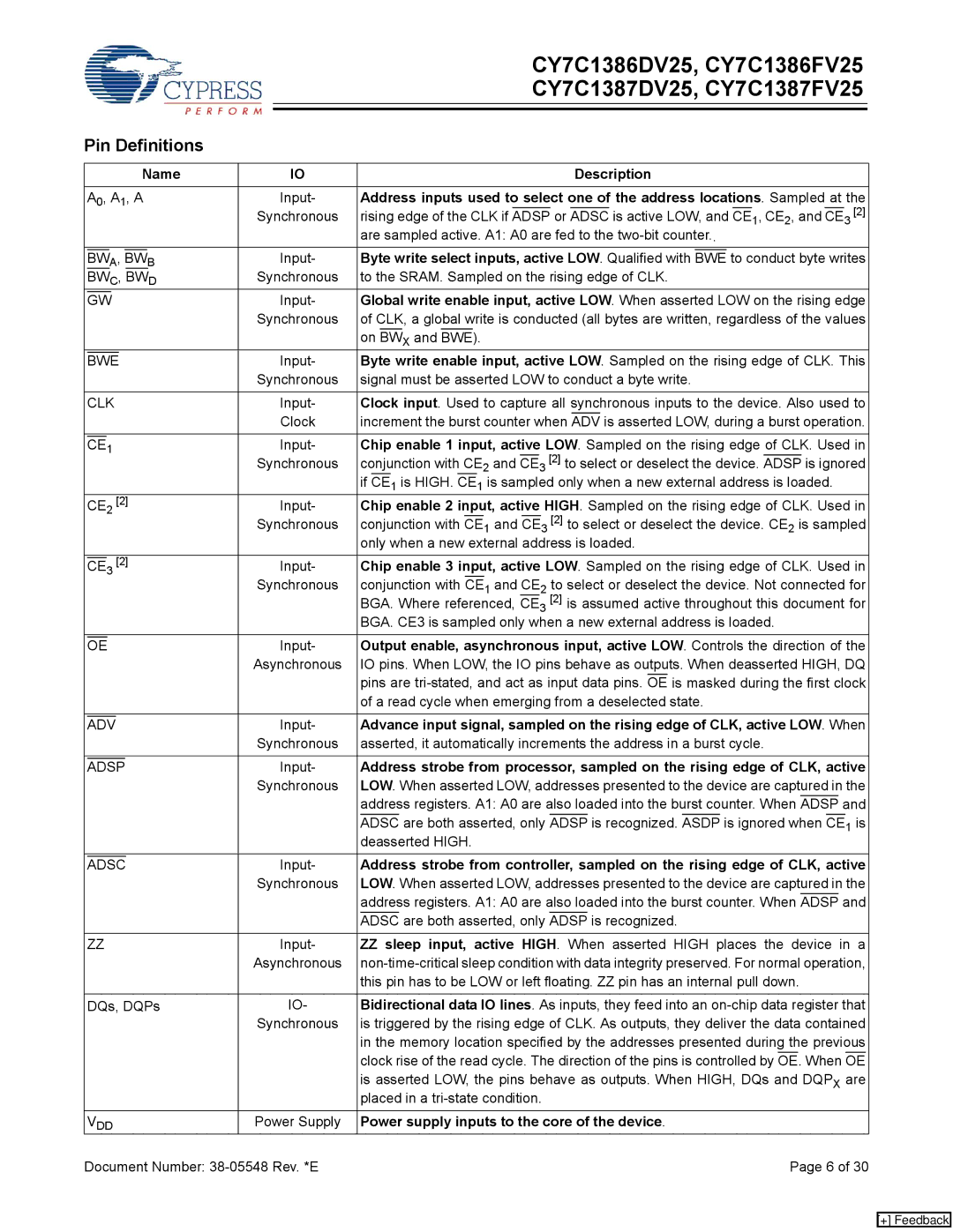
Pin Definitions |
|
|
|
|
| CY7C1387DV25, CY7C1387FV25 | |||||||||||||||
|
|
| |||||||||||||||||||
|
|
|
|
|
|
|
|
|
| ||||||||||||
|
|
|
|
|
|
|
|
|
| ||||||||||||
|
|
|
|
|
|
|
|
|
| ||||||||||||
|
|
|
|
|
|
|
|
|
|
|
|
|
|
|
|
| |||||
|
|
|
|
|
|
|
|
|
| Name |
|
| IO |
|
| Description | |||||
|
|
|
|
|
| ||||||||||||||||
| A0, A1, A |
|
| Input- | Address inputs used to select one of the address locations. Sampled at the | ||||||||||||||||
|
|
|
|
|
|
|
|
|
|
|
| Synchronous | rising edge of the CLK if ADSP or ADSC is active LOW, and CE1, CE2, and | CE | 3 [2] | ||||||
|
|
|
|
|
|
|
|
|
|
|
|
|
|
| are sampled active. A1: A0 are fed to the | ||||||
|
|
|
| A, |
|
|
| B |
|
| Input- | Byte write select inputs, active LOW. Qualified with |
| to conduct byte writes | |||||||
| BW | BW |
|
| BWE | ||||||||||||||||
| BWC, BWD | Synchronous | to the SRAM. Sampled on the rising edge of CLK. | ||||||||||||||||||
|
|
|
|
|
|
|
|
|
|
|
| Input- | Global write enable input, active LOW. When asserted LOW on the rising edge | ||||||||
| GW |
|
| ||||||||||||||||||
|
|
|
|
|
|
|
|
|
|
|
| Synchronous | of CLK, a global write is conducted (all bytes are written, regardless of the values | ||||||||
|
|
|
|
|
|
|
|
|
|
|
|
|
|
| on BWX and BWE). | ||||||
|
|
|
|
|
|
|
|
|
|
|
| Input- | Byte write enable input, active LOW. Sampled on the rising edge of CLK. This | ||||||||
| BWE |
|
| ||||||||||||||||||
|
|
|
|
|
|
|
|
|
|
|
| Synchronous | signal must be asserted LOW to conduct a byte write. | ||||||||
|
|
|
|
|
| ||||||||||||||||
| CLK |
|
| Input- | Clock input. Used to capture all synchronous inputs to the device. Also used to | ||||||||||||||||
|
|
|
|
|
|
|
|
|
|
|
|
|
| Clock | increment the burst counter when ADV is asserted LOW, during a burst operation. | ||||||
|
|
|
|
|
|
|
|
|
| ||||||||||||
|
| 1 |
|
|
|
|
| Input- | Chip enable 1 input, active LOW. Sampled on the rising edge of CLK. Used in | ||||||||||||
| CE |
|
| ||||||||||||||||||
|
|
|
|
|
|
|
|
|
|
|
| Synchronous | conjunction with CE2 and CE3 [2] to select or deselect the device. ADSP is ignored | ||||||||
|
|
|
|
|
|
|
|
|
|
|
|
|
|
| if CE1 is HIGH. | CE | 1 is sampled only when a new external address is loaded. | ||||
| CE2 [2] |
|
| Input- | Chip enable 2 input, active HIGH. Sampled on the rising edge of CLK. Used in | ||||||||||||||||
|
|
|
|
|
|
|
|
|
|
|
| Synchronous | conjunction with CE1 and CE3 [2] to select or deselect the device. CE2 is sampled | ||||||||
|
|
|
|
|
|
|
|
|
|
|
|
|
|
| only when a new external address is loaded. | ||||||
|
|
|
|
|
|
| |||||||||||||||
|
| 3 [2] |
|
| Input- | Chip enable 3 input, active LOW. Sampled on the rising edge of CLK. Used in | |||||||||||||||
| CE |
|
| ||||||||||||||||||
|
|
|
|
|
|
|
|
|
|
|
| Synchronous | conjunction with CE1 and CE2 to select or deselect the device. Not connected for | ||||||||
|
|
|
|
|
|
|
|
|
|
|
|
|
|
| BGA. Where referenced, CE3 [2] is assumed active throughout this document for | ||||||
|
|
|
|
|
|
|
|
|
|
|
|
|
|
| BGA. CE3 is sampled only when a new external address is loaded. | ||||||
|
|
|
|
|
|
|
|
|
| ||||||||||||
|
|
|
|
|
|
|
|
| Input- | Output enable, asynchronous input, active LOW. Controls the direction of the | |||||||||||
| OE |
|
| ||||||||||||||||||
|
|
|
|
|
|
|
|
|
|
|
| Asynchronous | IO pins. When LOW, the IO pins behave as outputs. When deasserted HIGH, DQ | ||||||||
|
|
|
|
|
|
|
|
|
|
|
|
|
|
| pins are | ||||||
|
|
|
|
|
|
|
|
|
|
|
|
|
|
| of a read cycle when emerging from a deselected state. | ||||||
|
|
|
|
|
|
|
|
| |||||||||||||
|
|
|
|
|
|
|
|
|
|
| Input- | Advance input signal, sampled on the rising edge of CLK, active LOW. When | |||||||||
| ADV |
|
| ||||||||||||||||||
|
|
|
|
|
|
|
|
|
|
|
| Synchronous | asserted, it automatically increments the address in a burst cycle. | ||||||||
|
|
|
|
|
|
|
| ||||||||||||||
|
|
|
|
|
|
|
|
|
|
|
|
| Input- | Address strobe from processor, sampled on the rising edge of CLK, active | |||||||
| ADSP |
|
| ||||||||||||||||||
|
|
|
|
|
|
|
|
|
|
|
| Synchronous | LOW. When asserted LOW, addresses presented to the device are captured in the | ||||||||
|
|
|
|
|
|
|
|
|
|
|
|
|
|
| address registers. A1: A0 are also loaded into the burst counter. When ADSP and | ||||||
|
|
|
|
|
|
|
|
|
|
|
|
|
|
| ADSC are both asserted, only ADSP is recognized. ASDP is ignored when CE1 is | ||||||
|
|
|
|
|
|
|
|
|
|
|
|
|
|
| deasserted HIGH. | ||||||
|
|
|
|
|
|
| |||||||||||||||
|
|
|
|
|
|
|
|
|
|
|
|
| Input- | Address strobe from controller, sampled on the rising edge of CLK, active | |||||||
| ADSC |
|
| ||||||||||||||||||
|
|
|
|
|
|
|
|
|
|
|
| Synchronous | LOW. When asserted LOW, addresses presented to the device are captured in the | ||||||||
|
|
|
|
|
|
|
|
|
|
|
|
|
|
| address registers. A1: A0 are also loaded into the burst counter. When ADSP and | ||||||
|
|
|
|
|
|
|
|
|
|
|
|
|
|
| ADSC are both asserted, only ADSP is recognized. | ||||||
|
|
|
|
|
| ||||||||||||||||
| ZZ |
|
| Input- | ZZ sleep input, active HIGH. When asserted HIGH places the device in a | ||||||||||||||||
|
|
|
|
|
|
|
|
|
|
|
| Asynchronous | |||||||||
|
|
|
|
|
|
|
|
|
|
|
|
|
|
| this pin has to be LOW or left floating. ZZ pin has an internal pull down. | ||||||
|
|
|
|
|
| ||||||||||||||||
| DQs, DQPs |
|
| IO- | Bidirectional data IO lines. As inputs, they feed into an | ||||||||||||||||
|
|
|
|
|
|
|
|
|
|
|
| Synchronous | is triggered by the rising edge of CLK. As outputs, they deliver the data contained | ||||||||
|
|
|
|
|
|
|
|
|
|
|
|
|
|
| in the memory location specified by the addresses presented during the previous | ||||||
|
|
|
|
|
|
|
|
|
|
|
|
|
|
| clock rise of the read cycle. The direction of the pins is controlled by OE. When OE | ||||||
|
|
|
|
|
|
|
|
|
|
|
|
|
|
| is asserted LOW, the pins behave as outputs. When HIGH, DQs and DQPX are | ||||||
|
|
|
|
|
|
|
|
|
|
|
|
|
|
| placed in a | ||||||
|
|
|
| ||||||||||||||||||
| VDD | Power Supply | Power supply inputs to the core of the device. | ||||||||||||||||||
Document Number: |
|
|
|
| Page 6 of 30 | ||||||||||||||||
[+] Feedback