CY7C1386DV25, CY7C1386FV25 CY7C1387DV25, CY7C1387FV25
The write signals (GW, BWE, and BWX) and ADV inputs are ignored during this first cycle.
ADSP triggered write accesses require two clock cycles to complete. If GW is asserted LOW on the second clock rise, the data presented to the DQx inputs is written into the corresponding address location in the memory core. If GW is HIGH, then the write operation is controlled by BWE and BWX signals.
The CY7C1386DV25/CY7C1387DV25/CY7C1386FV25/ CY7C1387FV25 provides byte write capability that is described in the write cycle description table. Asserting the byte write enable input (BWE) with the selected byte write input will selectively write to only the desired bytes. Bytes not selected during a byte write operation will remain unaltered. A synchronous self timed write mechanism has been provided to simplify the write operations.
The CY7C1386DV25/CY7C1387DV25/CY7C1386FV25/ CY7C1387FV25 is a common IO device, the output enable (OE) must be deasserted HIGH before presenting data to the DQ inputs. Doing so will
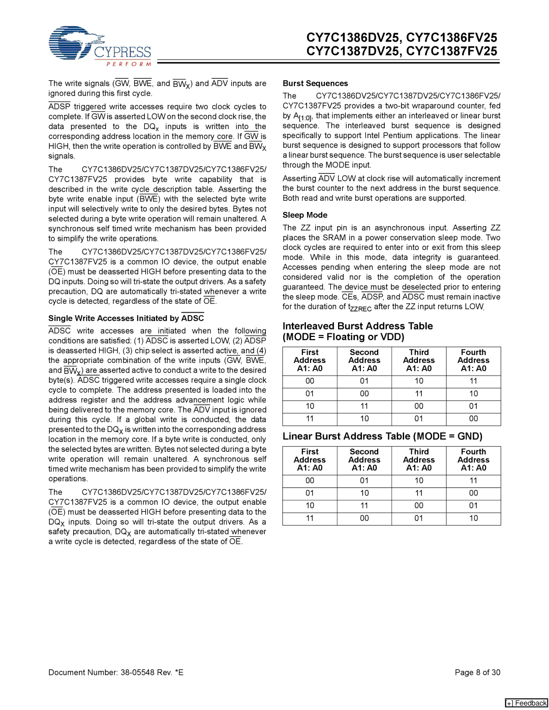
Burst Sequences
The CY7C1386DV25/CY7C1387DV25/CY7C1386FV25/ CY7C1387FV25 provides a
Asserting ADV LOW at clock rise will automatically increment the burst counter to the next address in the burst sequence. Both read and write burst operations are supported.
Sleep Mode
The ZZ input pin is an asynchronous input. Asserting ZZ places the SRAM in a power conservation sleep mode. Two clock cycles are required to enter into or exit from this sleep mode. While in this mode, data integrity is guaranteed. Accesses pending when entering the sleep mode are not considered valid nor is the completion of the operation guaranteed. The device must be deselected prior to entering the sleep mode. CEs, ADSP, and ADSC must remain inactive for the duration of tZZREC after the ZZ input returns LOW.
Single Write Accesses Initiated by ADSC
ADSC write accesses are initiated when the following conditions are satisfied: (1) ADSC is asserted LOW, (2) ADSP is deasserted HIGH, (3) chip select is asserted active, and (4) the appropriate combination of the write inputs (GW, BWE, and BWX) are asserted active to conduct a write to the desired byte(s). ADSC triggered write accesses require a single clock cycle to complete. The address presented is loaded into the address register and the address advancement logic while being delivered to the memory core. The ADV input is ignored during this cycle. If a global write is conducted, the data presented to the DQX is written into the corresponding address location in the memory core. If a byte write is conducted, only the selected bytes are written. Bytes not selected during a byte write operation will remain unaltered. A synchronous self timed write mechanism has been provided to simplify the write operations.
The CY7C1386DV25/CY7C1387DV25/CY7C1386FV25/ CY7C1387FV25 is a common IO device, the output enable (OE) must be deasserted HIGH before presenting data to the DQX inputs. Doing so will
Interleaved Burst Address Table (MODE = Floating or VDD)
First | Second | Third | Fourth |
Address | Address | Address | Address |
A1: A0 | A1: A0 | A1: A0 | A1: A0 |
00 | 01 | 10 | 11 |
|
|
|
|
01 | 00 | 11 | 10 |
|
|
|
|
10 | 11 | 00 | 01 |
|
|
|
|
11 | 10 | 01 | 00 |
|
|
|
|
Linear Burst Address Table (MODE = GND)
First | Second | Third | Fourth |
Address | Address | Address | Address |
A1: A0 | A1: A0 | A1: A0 | A1: A0 |
00 | 01 | 10 | 11 |
|
|
|
|
01 | 10 | 11 | 00 |
|
|
|
|
10 | 11 | 00 | 01 |
|
|
|
|
11 | 00 | 01 | 10 |
|
|
|
|
Document Number: | Page 8 of 30 |
[+] Feedback