CY7C1386DV25, CY7C1386FV25
CY7C1387DV25, CY7C1387FV25
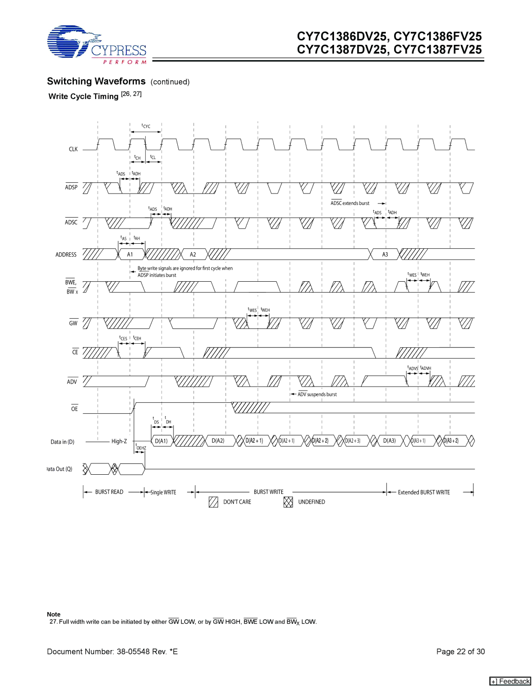
Switching Waveforms (continued)
Write Cycle Timing [26, 27]
t CYC
CLK
tCH tCL
tADS tADH
ADSP
tADS tADH
ADSC
tAS tAH
ADDRESS  A1
A1 
 A2
A2
Byte write signals are ignored for first cycle when
ADSP initiates burst
ADSC extends burst
tADS tADH
A3
tWES tWEH
BWE,
BW X
tWES tWEH
GW
| tCES | tCEH |
|
CE |
|
|
|
ADV |
|
|
|
OE |
|
|
|
|
| t | t |
|
| DS | DH |
Data in (D) | D(A1) | ||
|
| tOEHZ |
|
Data Out (Q) |
|
|
|
tADVS tADVH
![]() ADV suspends burst
ADV suspends burst
D(A2) | D(A2 + 1) | D(A2 + 3) | D(A3) | D(A3 + 1) |
BURST READ | Single WRITE |
BURST WRITE
DON’T CARE
![]()
![]()
![]() Extended BURST WRITE
Extended BURST WRITE
UNDEFINED
Note
27. Full width write can be initiated by either GW LOW, or by GW HIGH, BWE LOW and BWX LOW.
Document Number: | Page 22 of 30 |
[+] Feedback