CY7C1386DV25, CY7C1386FV25
CY7C1387DV25, CY7C1387FV25
TAP AC Switching Characteristics
Over the Operating Range [11, 12]
Parameter | Description | Min. | Max. | Unit |
Clock |
|
|
|
|
|
|
|
|
|
tTCYC | TCK Clock Cycle Time | 50 |
| ns |
tTF | TCK Clock Frequency |
| 20 | MHz |
tTH | TCK Clock HIGH time | 20 |
| ns |
tTL | TCK Clock LOW time | 20 |
| ns |
Output Times |
|
|
|
|
tTDOV | TCK Clock LOW to TDO Valid |
| 10 | ns |
tTDOX | TCK Clock LOW to TDO Invalid | 0 |
| ns |
Setup Times |
|
|
|
|
tTMSS | TMS Setup to TCK Clock Rise | 5 |
| ns |
tTDIS | TDI Setup to TCK Clock Rise | 5 |
| ns |
tCS | Capture Setup to TCK Rise | 5 |
| ns |
Hold Times |
|
|
|
|
|
|
|
|
|
tTMSH | TMS Hold after TCK Clock Rise | 5 |
| ns |
tTDIH | TDI Hold after Clock Rise | 5 |
| ns |
tCH | Capture Hold after Clock Rise | 5 |
| ns |
TAP AC Test Conditions
Input pulse levels | VSS to 2.5V |
Input rise and fall time | 1 ns |
Input timing reference levels | 1.25V |
Output reference levels | 1.25V |
Test load termination supply voltage | 1.25V |
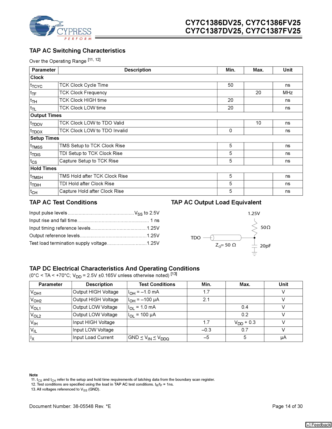
TAP AC Output Load Equivalent
1.25V
50Ω
TDO ![]()
ZO= 50 Ω |
|
|
|
|
| 20pF |
|
|
|
|
| ||
|
|
|
|
|
|
|
|
|
|
|
|
|
|
|
|
|
|
|
|
|
TAP DC Electrical Characteristics And Operating Conditions (0°C < TA < +70°C; VDD = 2.5V ±0.165V unless otherwise noted) [13]
Parameter | Description | Test Conditions | Min. | Max. | Unit |
VOH1 | Output HIGH Voltage | IOH = | 1.7 |
| V |
VOH2 | Output HIGH Voltage | IOH = | 2.1 |
| V |
VOL1 | Output LOW Voltage | IOL = 1.0 mA |
| 0.4 | V |
VOL2 | Output LOW Voltage | IOL = 100 µA |
| 0.2 | V |
VIH | Input HIGH Voltage |
| 1.7 | VDD + 0.3 | V |
VIL | Input LOW Voltage |
| 0.7 | V | |
IX | Input Load Current | GND < VIN < VDDQ | 5 | µA |
Note
11.tCS and tCH refer to the setup and hold time requirements of latching data from the boundary scan register.
12.Test conditions are specified using the load in TAP AC test conditions. tR/tF = 1ns.
13.All voltages referenced to VSS (GND).
Document Number: | Page 14 of 30 |
[+] Feedback