CY7C63413C


CY7C63513C


CY7C63613C


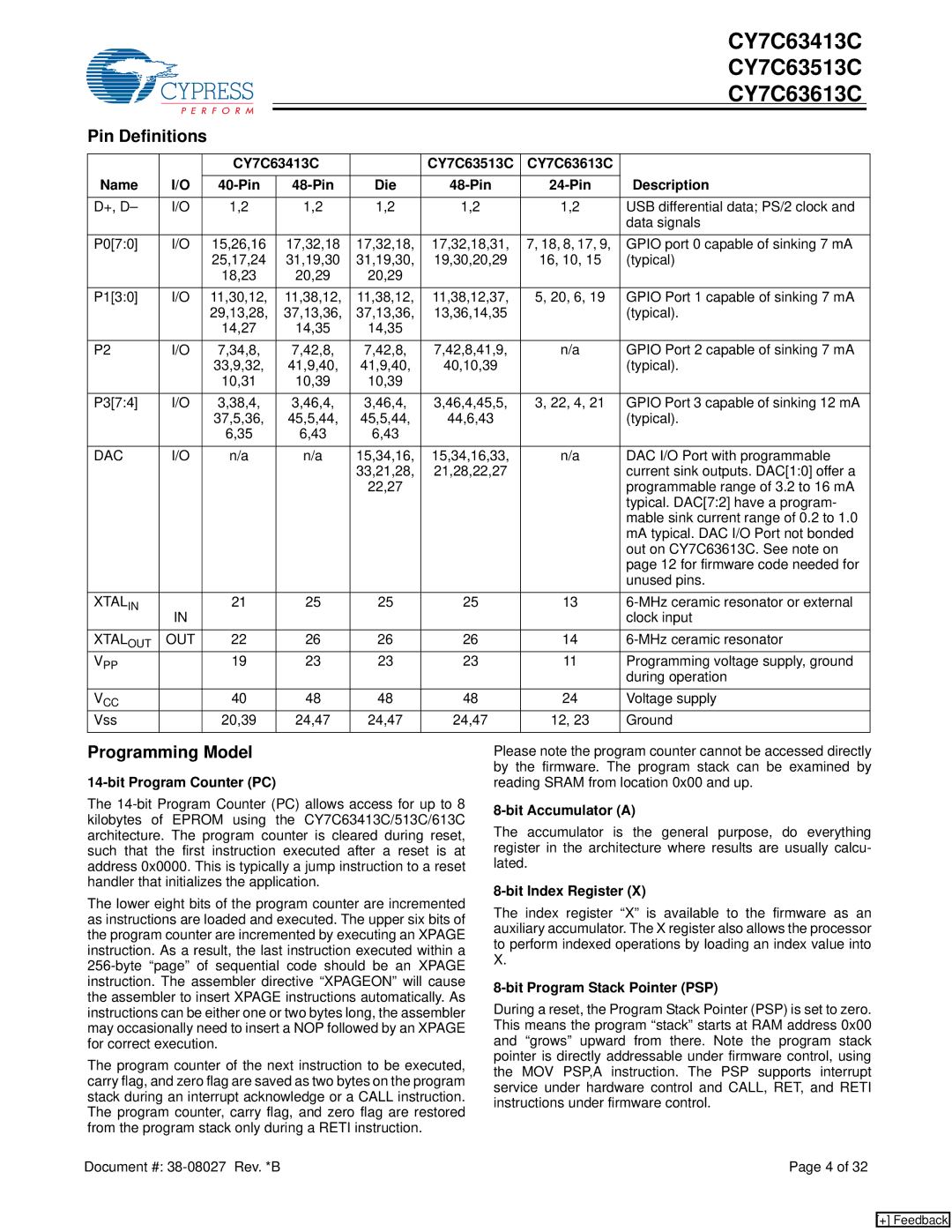
Pin Definitions


CY7C63413C


CY7C63513C

CY7C63613C


Name

I/O


40-Pin


48-Pin

Die

48-Pin

24-Pin

Description


D+, D–

I/O


1,2


1,2

1,2

1,2

1,2

USB differential data; PS/2 clock and


data signals


P0[7:0]

I/O


15,26,16


17,32,18

17,32,18,

17,32,18,31,

7, 18, 8, 17, 9,

GPIO port 0 capable of sinking 7 mA


25,17,24


31,19,30

31,19,30,

19,30,20,29

16, 10, 15

(typical)


18,23


20,29

20,29


P1[3:0]

I/O


11,30,12,


11,38,12,

11,38,12,

11,38,12,37,

5, 20, 6, 19

GPIO Port 1 capable of sinking 7 mA


29,13,28,


37,13,36,

37,13,36,

13,36,14,35


(typical).


14,27


14,35

14,35


P2

I/O


7,34,8,


7,42,8,

7,42,8,

7,42,8,41,9,

n/a

GPIO Port 2 capable of sinking 7 mA


33,9,32,


41,9,40,

41,9,40,

40,10,39


(typical).


10,31


10,39

10,39


P3[7:4]

I/O


3,38,4,


3,46,4,

3,46,4,

3,46,4,45,5,

3, 22, 4, 21

GPIO Port 3 capable of sinking 12 mA


37,5,36,


45,5,44,

45,5,44,

44,6,43


(typical).


6,35


6,43

6,43


DAC

I/O


n/a


n/a

15,34,16,

15,34,16,33,

n/a

DAC I/O Port with programmable


33,21,28,

21,28,22,27


current sink outputs. DAC[1:0] offer a


22,27


programmable range of 3.2 to 16 mA


typical. DAC[7:2] have a program-


mable sink current range of 0.2 to 1.0


mA typical. DAC I/O Port not bonded


out on CY7C63613C. See note on


page 12 for firmware code needed for


unused pins.


XTALIN

IN


21


25

25

25

13

6-MHz ceramic resonator or external


clock input


XTALOUT

OUT


22


26

26

26

14

6-MHz ceramic resonator


VPP


19


23

23

23

11

Programming voltage supply, ground


during operation


VCC


40


48

48

48

24

Voltage supply


Vss


20,39


24,47

24,47

24,47

12, 23

Ground


Programming Model

14-bit Program Counter (PC)

The 14-bit Program Counter (PC) allows access for up to 8 kilobytes of EPROM using the CY7C63413C/513C/613C architecture. The program counter is cleared during reset, such that the first instruction executed after a reset is at address 0x0000. This is typically a jump instruction to a reset handler that initializes the application.

The lower eight bits of the program counter are incremented as instructions are loaded and executed. The upper six bits of the program counter are incremented by executing an XPAGE instruction. As a result, the last instruction executed within a 256-byte “page” of sequential code should be an XPAGE instruction. The assembler directive “XPAGEON” will cause the assembler to insert XPAGE instructions automatically. As instructions can be either one or two bytes long, the assembler may occasionally need to insert a NOP followed by an XPAGE for correct execution.

The program counter of the next instruction to be executed, carry flag, and zero flag are saved as two bytes on the program stack during an interrupt acknowledge or a CALL instruction. The program counter, carry flag, and zero flag are restored from the program stack only during a RETI instruction.

Please note the program counter cannot be accessed directly by the firmware. The program stack can be examined by reading SRAM from location 0x00 and up.

8-bit Accumulator (A)

The accumulator is the general purpose, do everything register in the architecture where results are usually calcu- lated.

8-bit Index Register (X)

The index register “X” is available to the firmware as an auxiliary accumulator. The X register also allows the processor to perform indexed operations by loading an index value into X.

8-bit Program Stack Pointer (PSP)

During a reset, the Program Stack Pointer (PSP) is set to zero. This means the program “stack” starts at RAM address 0x00 and “grows” upward from there. Note the program stack pointer is directly addressable under firmware control, using the MOV PSP,A instruction. The PSP supports interrupt service under hardware control and CALL, RET, and RETI instructions under firmware control.

Document #: 38-08027 Rev. *B

Page 4 of 32

[+] Feedback

Page 4
Image 4
Cypress CY7C63513C, CY7C63613C, CY7C63413C manual Pin Definitions, Programming Model

CY7C63613C, CY7C63413C, CY7C63513C specifications

The Cypress CY7C63513C, CY7C63413C, and CY7C63613C are versatile programmable logic devices that are part of the Cypress family of microcontrollers designed for diverse applications. These devices are particularly well-suited for embedded systems, consumer electronics, and industrial control systems due to their robust features and technologies.

One of the standout characteristics of these devices is their programmable architecture, which allows for flexible design implementations. The CY7C63513C features 32 programmable I/O pins and an 8-bit microcontroller core, which provides ample resource allocation for various input/output operations. The device supports various communication interfaces, including SPI and I2C, enabling seamless integration into different system configurations.

The CY7C63413C is a highly adaptable component, offering similar features but with an enhanced flexibility in its I/O configuration, making it ideal for applications that require quick prototyping and development cycles. Its extensive instruction set allows for more complex processing tasks, catering to advanced applications in automation and signal processing.

On the other hand, the CY7C63613C provides an advanced level of integration with built-in support for multiple power management modes. This feature is crucial in modern battery-operated devices where energy conservation is a primary concern. Its low-power operation enhances the usability in portable applications while still maintaining performance.

In terms of performance, all three devices boast high-speed operation, with clock frequencies reaching up to 24 MHz. This ensures that they can efficiently handle tasks that require real-time processing, such as sensor data management and control algorithms. The devices are also equipped with an on-chip EEPROM and RAM, allowing for data storage and quick retrieval.

In addition to their performance characteristics, the CY7C63513C, CY7C63413C, and CY7C63613C are designed with reliability in mind. They incorporate robust error detection and correction features, ensuring data integrity during operation. This reliability is essential for critical applications, such as automotive systems and industrial automation.

Overall, the Cypress CY7 series presents an appealing solution for developers looking for a blend of flexibility, performance, and reliability in their embedded designs. Their programmability and support for multiple communication protocols make them a formidable choice in today’s fast-paced technological landscape, paving the way for innovative applications across various industries.