CY7C68013A, CY7C68014A CY7C68015A, CY7C68016A

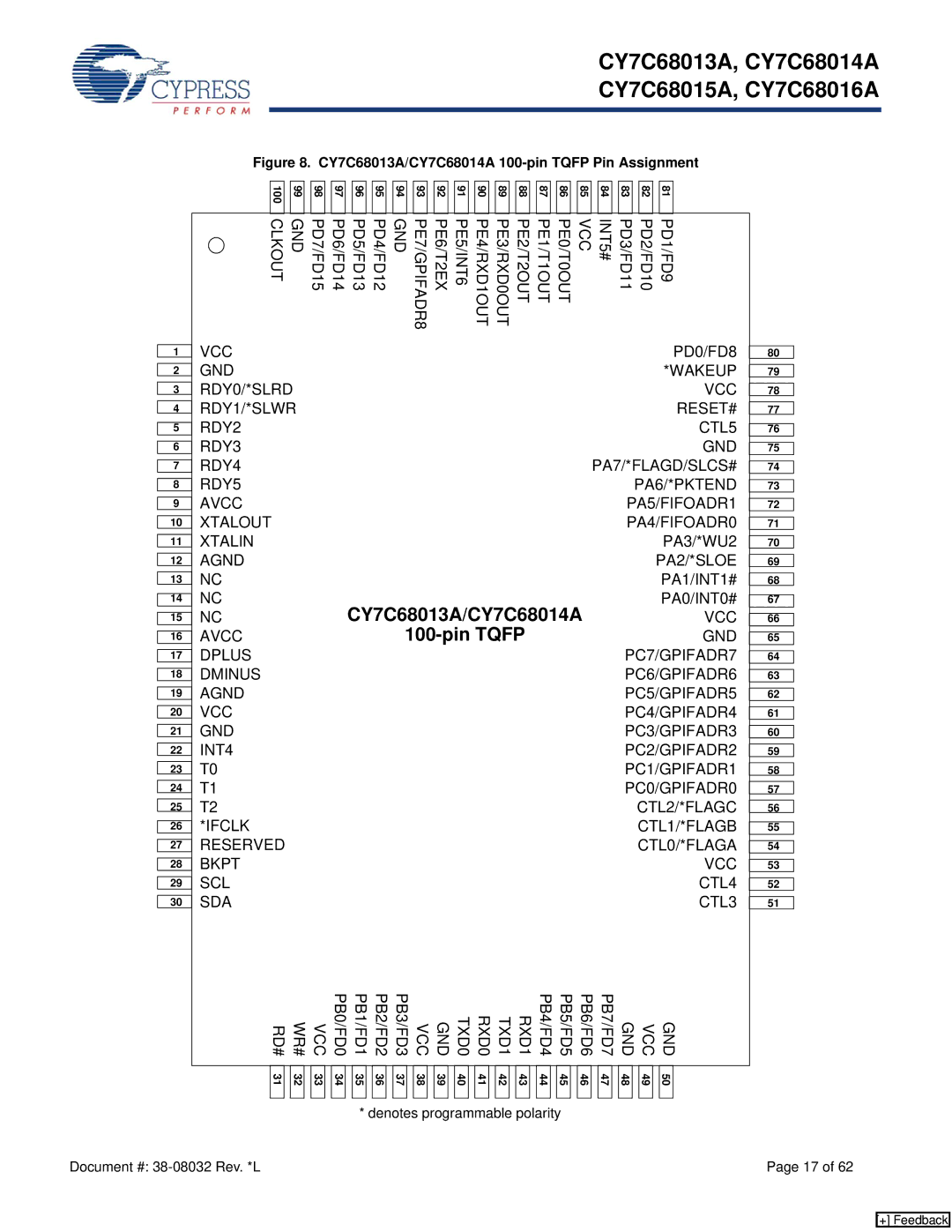
Figure 8. CY7C68013A/CY7C68014A 100-pin TQFP Pin Assignment


100


99


98


97


96


95


94


93


92


91


90


89


88


87


86


85


84


83


82


81


PD7/FD15 GND CLKOUT

PD6/FD14


PD5/FD13

PD4/FD12

PE7/GPIFADR8 GND

PE6/T2EX

PE5/INT6

PE4/RXD1OUT

PE3/RXD0OUT

PE2/T2OUT

PE1/T1OUT

PE0/T0OUT

INT5# VCC

PD3/FD11


PD2/FD10


PD1/FD9


VCC


PD0/FD8

1


GND


*WAKEUP

2


RDY0/*SLRD


VCC

3


RDY1/*SLWR


RESET#

4


RDY2


CTL5

5


RDY3


GND

6


RDY4


PA7/*FLAGD/SLCS#

7


RDY5


PA6/*PKTEND

8


AVCC


PA5/FIFOADR1

9


XTALOUT


PA4/FIFOADR0

10


XTALIN


PA3/*WU2

11


AGND


PA2/*SLOE

12


NC


PA1/INT1#

13


NC


PA0/INT0#

14


CY7C68013A/CY7C68014A


NC


VCC

15


AVCC


100-pin TQFP


GND

16


DPLUS


PC7/GPIFADR7

17


DMINUS


PC6/GPIFADR6

18


AGND


PC5/GPIFADR5

19


VCC


PC4/GPIFADR4

20


GND


PC3/GPIFADR3

21


INT4


PC2/GPIFADR2

22


T0


PC1/GPIFADR1

23


T1


PC0/GPIFADR0

24


25


T2


CTL2/*FLAGC


*IFCLK


CTL1/*FLAGB

26


RESERVED


CTL0/*FLAGA

27


BKPT


VCC

28


SCL


CTL4

29


SDA


CTL3

30


RD#

WR#

VCC

PB0/FD0

PB1/FD1

PB2/FD2

PB3/FD3

VCC

GND

TXD0

RXD0

TXD1

RXD1

PB4/FD4

PB5/FD5

PB6/FD6

PB7/FD7

GND

VCC

GND


31


32


33


34


35


36


37


38


39


40


41


42


43


44


45


46


47


48


49


50


* denotes programmable polarity

80

79

78

77

76

75

74

73

72

71

70

69

68

67

66

65

64

63

62

61

60

59

58

57

56

55

54

53

52

51

Document #: 38-08032 Rev. *L

Page 17 of 62

[+] Feedback

Page 17
Image 17
Cypress CY7C68015A, CY7C68016A manual CY7C68013A/CY7C68014A

CY7C68016A, CY7C68014A, CY7C68015A, CY7C68013 specifications

The Cypress CY7C68013, CY7C68015A, CY7C68014A, and CY7C68016A are part of Cypress Semiconductor's EZ-USB family of microcontrollers, known for their high performance and flexibility in USB applications. These devices are primarily used for USB interfacing and have gained popularity in various industries due to their robust features and capabilities.

One of the main features of the CY7C68013 is its Dual FIFO architecture, allowing for efficient data transfer between USB and the system memory. This feature optimizes throughput and reduces CPU overhead, making it an excellent choice for applications that require high-speed data exchange, such as video streaming, data acquisition, and industrial automation. The device is equipped with a USB 2.0 interface which supports full-speed operation at 12 Mbps, ensuring compatibility with a wide range of USB devices.

The CY7C68015A, a similar variant, offers additional memory options, providing users with the flexibility to select the necessary capacity for their specific applications. This part is particularly useful in scenarios that demand more users or higher data storage, making it ideal for complex USB peripherals like printers and multifunction devices. Moreover, it includes a unique capability of upgradeable firmware, ensuring that the device remains relevant and functional as technology evolves.

In contrast, the CY7C68014A stands out with its support for isochronous data transfers, making it suitable for real-time applications that require timely data delivery. This is particularly important in audio and video applications where delays can impact performance. The device incorporates advanced power management features, allowing it to operate efficiently both in low and high-power modes.

Lastly, the CY7C68016A integrates enhanced security features, positioning it as an ideal choice for applications that require data integrity and protection against unauthorized access. It supports various encryption standards and provides secure boot capabilities, making it suitable for secure environments such as financial transactions and sensitive data processing.

In summary, the CY7C68013, CY7C68015A, CY7C68014A, and CY7C68016A microcontrollers offer a versatile suite of features that cater to a wide array of USB applications. Their design emphasizes performance, flexibility, and security, making them essential components in today's rapidly evolving technology landscape. Whether in consumer electronics, industrial automation, or specialized applications, these devices provide the reliability and efficiency that engineers and developers require.