CY8C20x36/46/66, CY8C20396
48-Pin QFN OCD
The
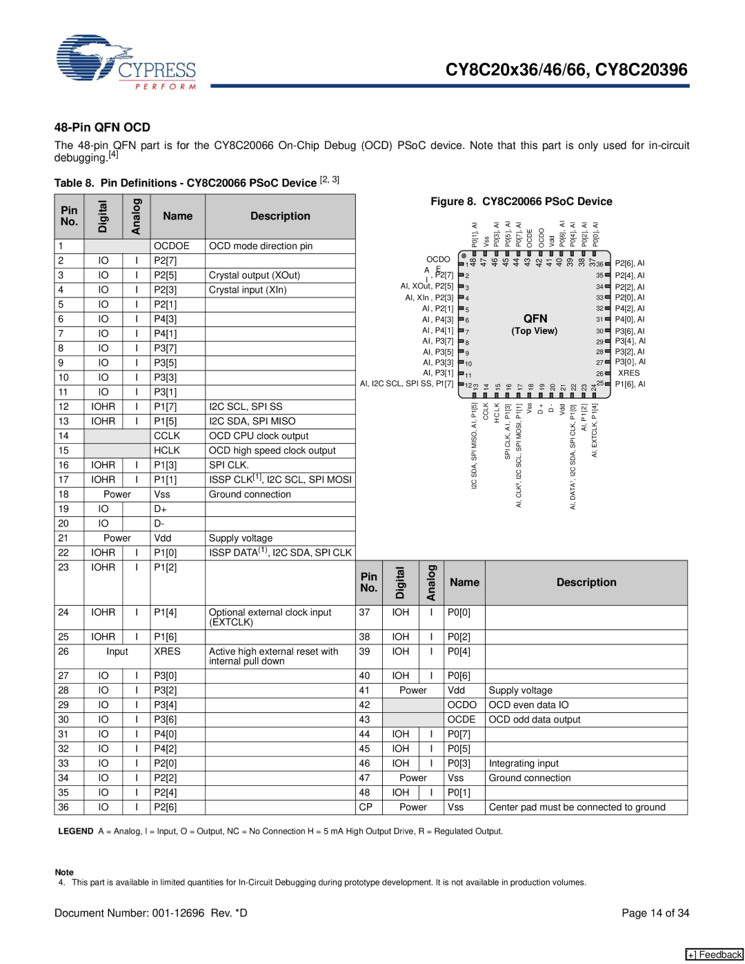
Table 8. Pin Definitions - CY8C20066 PSoC Device [2, 3]
Pin | Digital |
| Analog | Name | Description |
No. |
|
|
| ||
|
|
|
|
| |
|
|
|
|
|
|
1 |
|
|
| OCDOE | OCD mode direction pin |
2 | IO |
| I | P2[7] |
|
3 | IO |
| I | P2[5] | Crystal output (XOut) |
4 | IO |
| I | P2[3] | Crystal input (XIn) |
5 | IO |
| I | P2[1] |
|
6 | IO |
| I | P4[3] |
|
7 | IO |
| I | P4[1] |
|
8 | IO |
| I | P3[7] |
|
9 | IO |
| I | P3[5] |
|
10 | IO |
| I | P3[3] |
|
11 | IO |
| I | P3[1] |
|
12 | IOHR |
| I | P1[7] | I2C SCL, SPI SS |
13 | IOHR |
| I | P1[5] | I2C SDA, SPI MISO |
14 |
|
|
| CCLK | OCD CPU clock output |
15 |
|
|
| HCLK | OCD high speed clock output |
16 | IOHR |
| I | P1[3] | SPI CLK. |
17 | IOHR |
| I | P1[1] | ISSP CLK[1], I2C SCL, SPI MOSI |
18 | Power | Vss | Ground connection | ||
19 | IO |
|
| D+ |
|
20 | IO |
|
| D- |
|
21 | Power | Vdd | Supply voltage | ||
22 | IOHR |
| I | P1[0] | ISSP DATA(1), I2C SDA, SPI CLK |
23 | IOHR |
| I | P1[2] |
|
24 | IOHR |
| I | P1[4] | Optional external clock input |
|
|
|
|
| (EXTCLK) |
25 | IOHR |
| I | P1[6] |
|
26 | Input |
| XRES | Active high external reset with | |
|
|
|
|
| internal pull down |
27 | IO |
| I | P3[0] |
|
28 | IO |
| I | P3[2] |
|
29 | IO |
| I | P3[4] |
|
30 | IO |
| I | P3[6] |
|
31 | IO |
| I | P4[0] |
|
32 | IO |
| I | P4[2] |
|
33 | IO |
| I | P2[0] |
|
34 | IO |
| I | P2[2] |
|
35 | IO |
| I | P2[4] |
|
36 | IO |
| I | P2[6] |
|
|
|
|
|
|
|
Figure 8. CY8C20066 PSoC Device
|
|
| P0[1], AI | Vss | P0[3], AI | P0[5 ], AI | P0[7], AI | OCDE | OCDO Vdd P0[6], AI | P0[4], AI | P0[2], AI | P0[0], AI |
|
| ||||||||||||
OCDO |
|
|
|
|
|
|
|
|
|
|
|
|
|
|
|
|
|
|
|
|
|
|
|
|
| |
|
|
|
|
|
|
|
|
|
|
|
|
|
|
|
|
|
|
|
|
|
|
|
|
| ||
| 14847 |
| 46 |
| 45 44 |
| 43 |
| 42 41 40 |
| 39 |
| 38 |
| 37 | 36 |
| P2[6], AI | ||||||||
A | E |
|
|
|
|
|
|
|
|
| ||||||||||||||||
| 2 |
|
|
|
|
|
|
|
|
|
|
|
|
|
|
|
|
|
|
|
| 35 |
|
| ||
I | , P2[7] |
|
|
|
|
|
|
|
|
|
|
|
|
|
|
|
|
|
|
|
|
|
| P2[4], AI | ||
|
|
|
|
|
|
|
|
|
|
|
|
|
|
|
|
|
|
|
|
|
|
| 34 |
|
| |
AI, XOut, P2[5] |
| 3 |
|
|
|
|
|
|
|
|
|
|
|
|
|
|
|
|
|
|
|
|
| P2[2], AI | ||
|
|
|
|
|
|
|
|
|
|
|
|
|
|
|
|
|
|
|
|
| ||||||
AI, XIn , P2[3] |
| 4 |
|
|
|
|
|
|
|
|
|
|
|
|
|
|
|
|
|
|
|
| 33 |
| P2[0], AI | |
|
|
|
|
|
|
|
|
|
|
|
|
|
|
|
|
|
|
|
|
| ||||||
AI , P2[1] |
| 5 |
|
|
|
|
|
|
|
|
| QFN |
|
|
|
|
| 32 |
| P4[2], AI | ||||||
|
|
|
|
|
|
|
|
|
|
|
|
|
|
| ||||||||||||
AI, P4[3] |
| 6 |
|
|
|
|
|
|
|
|
|
|
|
|
|
| 31 |
| P4[0], AI | |||||||
|
|
|
|
|
|
|
|
|
|
|
|
|
|
| ||||||||||||
AI, P4[1] |
| 7 |
|
|
|
|
|
|
| (Top View) |
|
|
|
|
| 30 |
| P3[6], AI | ||||||||
|
|
|
|
|
|
|
|
|
|
|
|
| ||||||||||||||
AI, P3[7] |
| 8 |
|
|
|
|
|
|
|
|
|
|
|
|
|
|
|
|
|
|
|
| 29 |
| P3[4], AI | |
|
|
|
|
|
|
|
|
|
|
|
|
|
|
|
|
|
|
|
|
| ||||||
AI, P3[5] |
| 9 |
|
|
|
|
|
|
|
|
|
|
|
|
|
|
|
|
|
|
|
| 28 |
| P3[2], AI | |
|
|
|
|
|
|
|
|
|
|
|
|
|
|
|
|
|
|
|
|
| ||||||
AI, P3[3] |
| 10 |
|
|
|
|
|
|
|
|
|
|
|
|
|
|
|
|
|
|
|
| 27 |
| P3[0], AI | |
|
|
|
|
|
|
|
|
|
|
|
|
|
|
|
|
|
|
|
|
| ||||||
AI, P3[1] |
| 11 |
|
|
|
|
|
|
|
|
|
|
|
|
|
|
|
|
|
|
|
| 26 |
| XRES | |
|
|
|
|
|
|
|
|
|
|
|
|
|
|
|
|
|
|
|
|
| ||||||
AI, I2C SCL, SPI SS, P1[7] |
| 121314 | 15 16 | 17 18 19 20 21 22 23 24 | 25 |
| P1[6], AI | |||||||||||||||||||
|
| |||||||||||||||||||||||||
|
|
|
|
|
|
|
|
|
|
|
|
|
|
|
|
|
|
|
|
|
|
|
|
|
| |
|
|
|
|
|
|
|
|
|
|
|
|
|
|
|
|
|
|
|
|
|
|
|
|
|
| |
|
|
| I2C SDA, SPI MISO, AI, P1[5] | CCLK | H C LK | SPI CLK, A I, P1[3] | AI, CLK6, I2C SCL, SPI MOSI, P1[1] | Vss D + D - Vdd | AI, DATA1, I2C SDA, SPI CLK, P1[0] | AI, P1[2] | AI, EXTCLK, P1[4] |
|
| |||||||||||||
Pin | Digital | Analog | Name | Description |
No. |
|
| ||
|
|
|
| |
37 | IOH | I | P0[0] |
|
38 | IOH | I | P0[2] |
|
39 | IOH | I | P0[4] |
|
40 | IOH | I | P0[6] |
|
41 | Power | Vdd | Supply voltage | |
42 |
|
| OCDO | OCD even data IO |
|
| |||
43 |
|
| OCDE | OCD odd data output |
44 | IOH | I | P0[7] |
|
45 | IOH | I | P0[5] |
|
46 | IOH | I | P0[3] | Integrating input |
47 | Power | Vss | Ground connection | |
48 | IOH | I | P0[1] |
|
CP | Power | Vss | Center pad must be connected to ground | |
|
|
|
|
|
LEGEND A = Analog, I = Input, O = Output, NC = No Connection H = 5 mA High Output Drive, R = Regulated Output.
Note
4. This part is available in limited quantities for
Document Number: | Page 14 of 34 |
[+] Feedback