CY8C20x36/46/66, CY8C20396
AC SPI Specifications
The following table lists guaranteed maximum and minimum specifications for the entire voltage and temperature ranges.
Table 31. AC SPI Specifications
Symbol | Description | Conditions | Min | Typ | Max | Units |
FSPIM | Maximum Input Clock Frequency Selection, | Output clock frequency is half | – | – | 12 | MHz |
| Master 2.4V<Vdd<5.5V | of input clock rate. |
|
|
|
|
|
|
|
|
|
|
|
| Maximum Input Clock Frequency Selection, | Output clock frequency is half |
|
| 6 | MHz |
| Master(21)1.71V<Vdd<2.4V | of input clock rate |
|
|
|
|
|
|
|
|
|
|
|
FSPIS | Maximum Input Clock Frequency Selection, |
| – | – | 12 | MHz |
| Slave 2.4<Vdd<5.5V |
|
|
|
|
|
| Maximum Input Clock Frequency Selection, |
|
|
| 6 | MHz |
| Slave 1.71V<Vdd<2.4V |
|
|
|
|
|
TSS | Width of SS_ Negated Between Transmissions |
| 50 | – | – | ns |
AC I2C Specifications
The following table lists guaranteed maximum and minimum specifications for the entire voltage and temperature ranges.
Table 32. AC Characteristics of the I2C SDA and SCL Pins
Symbol | Description | Standard Mode | Fast Mode | Units | ||
Min | Max | Min | Max | |||
FSCLI2C | SCL Clock Frequency | 0 | 100 | 0 | 400 | kHz |
THDSTAI2C | Hold Time (repeated) START Condition. After this period, the first clock pulse is | 4.0 | – | 0.6 | – | μs |
| generated. |
|
|
|
|
|
TLOWI2C | LOW Period of the SCL Clock | 4.7 | – | 1.3 | – | μs |
THIGHI2C | HIGH Period of the SCL Clock | 4.0 | – | 0.6 | – | μs |
TSUSTAI2C | Setup Time for a Repeated START Condition | 4.7 | – | 0.6 | – | μs |
THDDATI2C | Data Hold Time | 0 | – | 0 | – | μs |
TSUDATI2C | Data Setup Time | 250 | – | 100[1 | – | ns |
|
|
|
| 0] |
|
|
|
|
|
|
|
|
|
TSUSTOI2C | Setup Time for STOP Condition | 4.0 | – | 0.6 | – | μs |
TBUFI2C | Bus Free Time Between a STOP and START Condition | 4.7 | – | 1.3 | – | μs |
TSPI2C | Pulse Width of spikes are suppressed by the input filter. | – | – | 0 | 50 | ns |
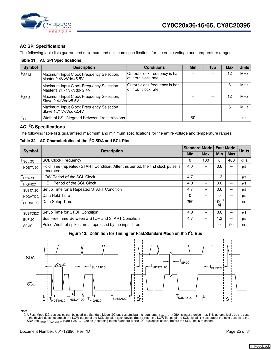
Figure 13. Definition for Timing for Fast/Standard Mode on the I2C Bus
SDA | TLOWI2C |
|
|
|
|
| TSUDATI2C |
| |
|
|
|
| |
SCL |
|
|
|
|
S | T | THDDATI2C | T | TSUSTAI2C |
| HDSTAI2C |
| HIGHI2C |
|

 THDSTAI2C
![]() Sr
Sr
TSPI2C |
| TBUFI2C |
|
| |
TSUSTOI2C | P | S |
|
Note
10.A
Document Number: | Page 25 of 34 |
[+] Feedback