CY8C20x36/46/66, CY8C20396
Absolute Maximum Ratings
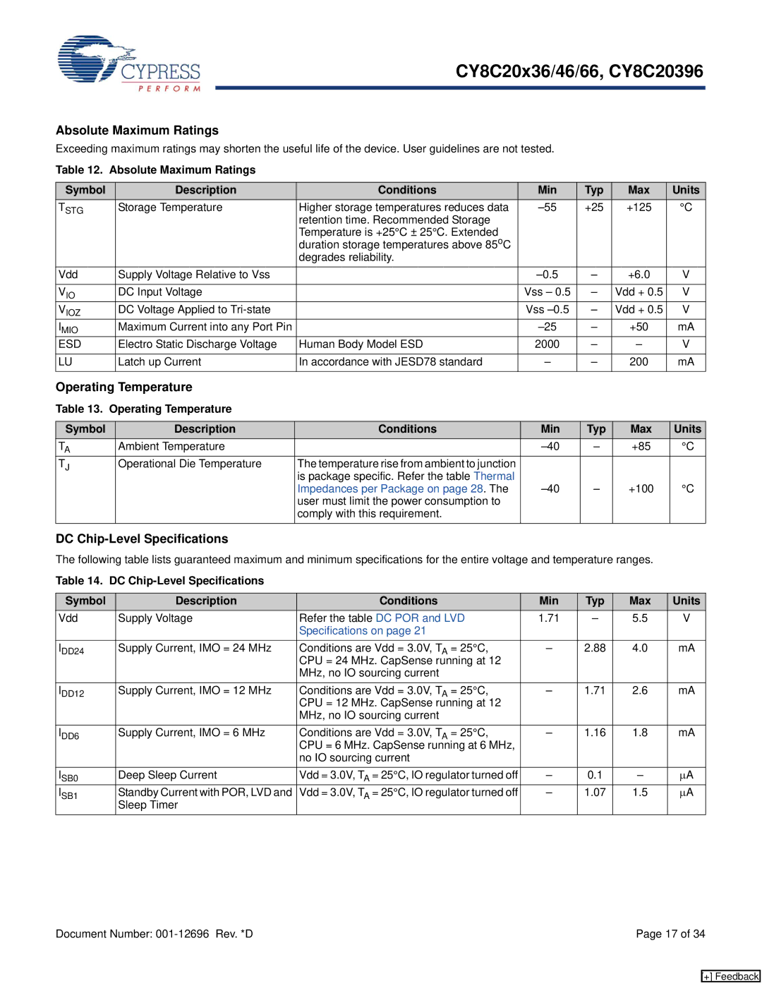
Exceeding maximum ratings may shorten the useful life of the device. User guidelines are not tested.
Table 12. Absolute Maximum Ratings
Symbol | Description | Conditions | Min | Typ | Max | Units |
TSTG | Storage Temperature | Higher storage temperatures reduces data | +25 | +125 | °C | |
|
| retention time. Recommended Storage |
|
|
|
|
|
| Temperature is +25°C ± 25°C. Extended |
|
|
|
|
|
| duration storage temperatures above 85oC |
|
|
|
|
|
| degrades reliability. |
|
|
|
|
Vdd | Supply Voltage Relative to Vss |
| – | +6.0 | V | |
|
|
|
|
|
|
|
VIO | DC Input Voltage |
| Vss – 0.5 | – | Vdd + 0.5 | V |
VIOZ | DC Voltage Applied to |
| Vss | – | Vdd + 0.5 | V |
IMIO | Maximum Current into any Port Pin |
| – | +50 | mA | |
ESD | Electro Static Discharge Voltage | Human Body Model ESD | 2000 | – | – | V |
|
|
|
|
|
|
|
LU | Latch up Current | In accordance with JESD78 standard | – | – | 200 | mA |
|
|
|
|
|
|
|
Operating Temperature
Table 13. Operating Temperature
Symbol | Description | Conditions | Min | Typ | Max | Units |
TA | Ambient Temperature |
| – | +85 | °C | |
TJ | Operational Die Temperature | The temperature rise from ambient to junction |
|
|
|
|
|
| is package specific. Refer the table Thermal |
|
|
|
|
|
| Impedances per Package on page 28. The | – | +100 | °C | |
|
| user must limit the power consumption to |
|
|
|
|
|
| comply with this requirement. |
|
|
|
|
DC Chip-Level Specifications
The following table lists guaranteed maximum and minimum specifications for the entire voltage and temperature ranges.
Table 14. DC
Symbol | Description | Conditions | Min | Typ | Max | Units |
Vdd | Supply Voltage | Refer the table DC POR and LVD | 1.71 | – | 5.5 | V |
|
| Specifications on page 21 |
|
|
|
|
IDD24 | Supply Current, IMO = 24 MHz | Conditions are Vdd = 3.0V, TA = 25°C, | – | 2.88 | 4.0 | mA |
|
| CPU = 24 MHz. CapSense running at 12 |
|
|
|
|
|
| MHz, no IO sourcing current |
|
|
|
|
IDD12 | Supply Current, IMO = 12 MHz | Conditions are Vdd = 3.0V, TA = 25°C, | – | 1.71 | 2.6 | mA |
|
| CPU = 12 MHz. CapSense running at 12 |
|
|
|
|
|
| MHz, no IO sourcing current |
|
|
|
|
IDD6 | Supply Current, IMO = 6 MHz | Conditions are Vdd = 3.0V, TA = 25°C, | – | 1.16 | 1.8 | mA |
|
| CPU = 6 MHz. CapSense running at 6 MHz, |
|
|
|
|
|
| no IO sourcing current |
|
|
|
|
ISB0 | Deep Sleep Current | Vdd = 3.0V, TA = 25°C, IO regulator turned off | – | 0.1 | – | μA |
ISB1 | Standby Current with POR, LVD and | Vdd = 3.0V, TA = 25°C, IO regulator turned off | – | 1.07 | 1.5 | μA |
| Sleep Timer |
|
|
|
|
|
Document Number: | Page 17 of 34 |
[+] Feedback
