CY8C20x36/46/66, CY8C20396
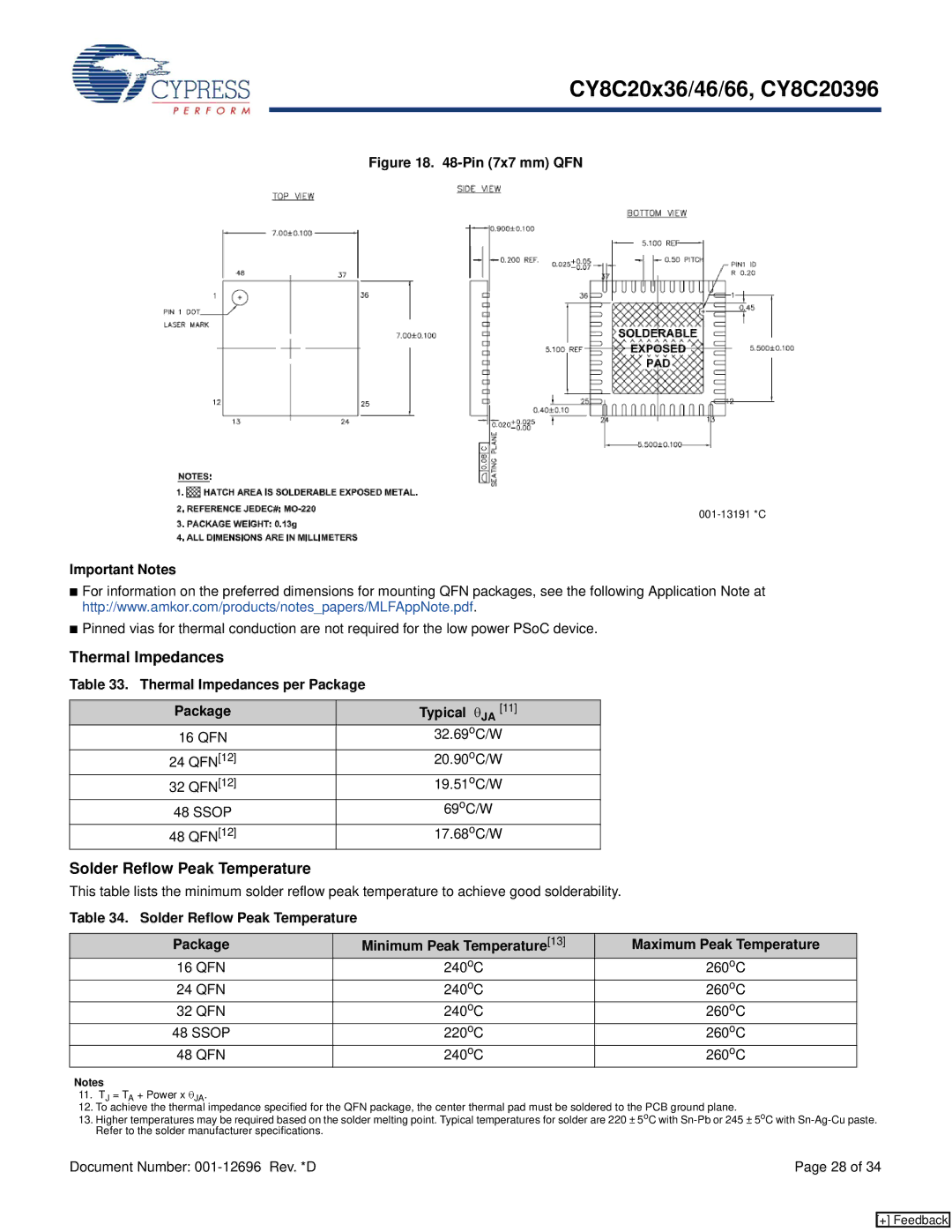
Figure 18. 48-Pin (7x7 mm) QFN
Important Notes
■For information on the preferred dimensions for mounting QFN packages, see the following Application Note at http://www.amkor.com/products/notes_papers/MLFAppNote.pdf.
■Pinned vias for thermal conduction are not required for the low power PSoC device.
Thermal Impedances
Table 33. Thermal Impedances per Package
Package | Typical θJA [11] |
16 QFN | 32.69oC/W |
24 QFN[12] | 20.90oC/W |
32 QFN[12] | 19.51oC/W |
48 SSOP | 69oC/W |
48 QFN[12] | 17.68oC/W |
Solder Reflow Peak Temperature
This table lists the minimum solder reflow peak temperature to achieve good solderability.
Table 34. Solder Reflow Peak Temperature
Package | Minimum Peak Temperature[13] | Maximum Peak Temperature |
16 QFN | 240oC | 260oC |
24 QFN | 240oC | 260oC |
32 QFN | 240oC | 260oC |
48 SSOP | 220oC | 260oC |
48 QFN | 240oC | 260oC |
Notes
11.TJ = TA + Power x θJA.
12.To achieve the thermal impedance specified for the QFN package, the center thermal pad must be soldered to the PCB ground plane.
13.Higher temperatures may be required based on the solder melting point. Typical temperatures for solder are 220 ± 5oC with
Document Number: | Page 28 of 34 |
[+] Feedback