CY8C20x36/46/66, CY8C20396
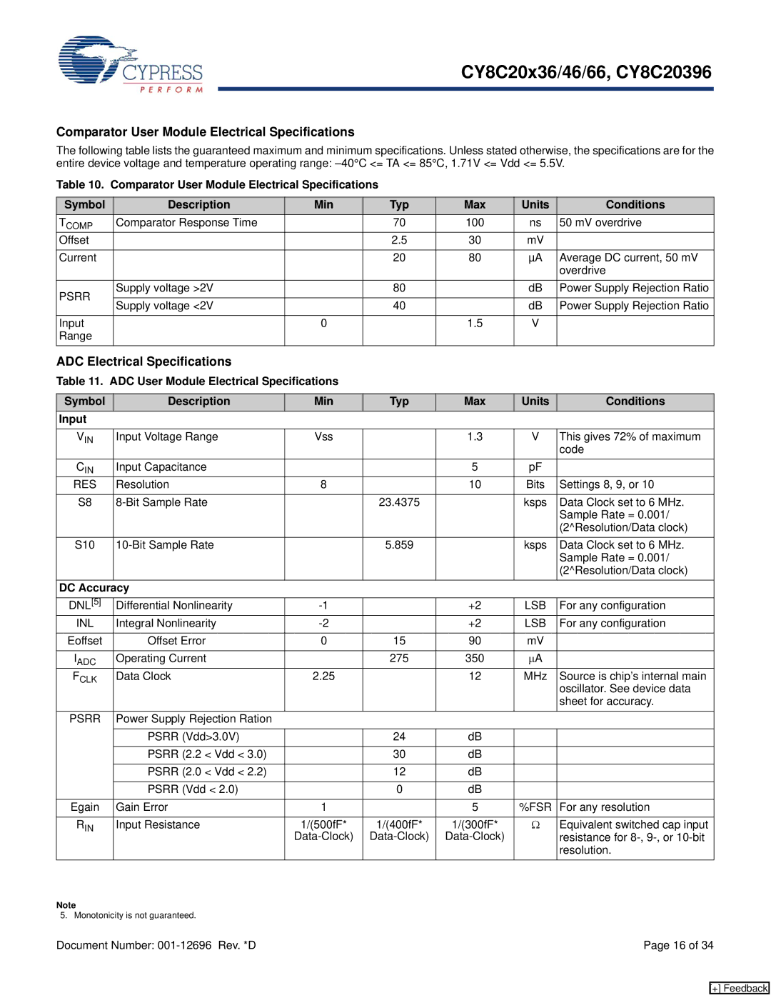
Comparator User Module Electrical Specifications
The following table lists the guaranteed maximum and minimum specifications. Unless stated otherwise, the specifications are for the entire device voltage and temperature operating range:
Table 10. Comparator User Module Electrical Specifications
Symbol | Description | Min | Typ | Max | Units | Conditions |
TCOMP | Comparator Response Time |
| 70 | 100 | ns | 50 mV overdrive |
Offset |
|
| 2.5 | 30 | mV |
|
|
|
|
|
|
|
|
Current |
|
| 20 | 80 | µA | Average DC current, 50 mV |
|
|
|
|
|
| overdrive |
PSRR | Supply voltage >2V |
| 80 |
| dB | Power Supply Rejection Ratio |
|
|
|
|
|
| |
Supply voltage <2V |
| 40 |
| dB | Power Supply Rejection Ratio | |
|
|
| ||||
|
|
|
|
|
|
|
Input |
| 0 |
| 1.5 | V |
|
Range |
|
|
|
|
|
|
ADC Electrical Specifications
Table 11. ADC User Module Electrical Specifications
Symbol | Description | Min | Typ | Max | Units | Conditions |
Input |
|
|
|
|
|
|
|
|
|
|
|
|
|
VIN | Input Voltage Range | Vss |
| 1.3 | V | This gives 72% of maximum |
|
|
|
|
|
| code |
CIN | Input Capacitance |
|
| 5 | pF |
|
RES | Resolution | 8 |
| 10 | Bits | Settings 8, 9, or 10 |
|
|
|
|
|
|
|
S8 |
| 23.4375 |
| ksps | Data Clock set to 6 MHz. | |
|
|
|
|
|
| Sample Rate = 0.001/ |
|
|
|
|
|
| (2^Resolution/Data clock) |
S10 |
| 5.859 |
| ksps | Data Clock set to 6 MHz. | |
|
|
|
|
|
| Sample Rate = 0.001/ |
|
|
|
|
|
| (2^Resolution/Data clock) |
DC Accuracy |
|
|
|
|
| |
DNL[5] | Differential Nonlinearity |
| +2 | LSB | For any configuration | |
INL | Integral Nonlinearity |
| +2 | LSB | For any configuration | |
|
|
|
|
|
|
|
Eoffset | Offset Error | 0 | 15 | 90 | mV |
|
|
|
|
|
|
|
|
IADC | Operating Current |
| 275 | 350 | μA |
|
FCLK | Data Clock | 2.25 |
| 12 | MHz | Source is chip’s internal main |
|
|
|
|
|
| oscillator. See device data |
|
|
|
|
|
| sheet for accuracy. |
PSRR | Power Supply Rejection Ration |
|
|
|
|
|
|
|
|
|
|
|
|
| PSRR (Vdd>3.0V) |
| 24 | dB |
|
|
|
|
|
|
|
|
|
| PSRR (2.2 < Vdd < 3.0) |
| 30 | dB |
|
|
|
|
|
|
|
|
|
| PSRR (2.0 < Vdd < 2.2) |
| 12 | dB |
|
|
|
|
|
|
|
|
|
| PSRR (Vdd < 2.0) |
| 0 | dB |
|
|
|
|
|
|
|
|
|
Egain | Gain Error | 1 |
| 5 | %FSR | For any resolution |
|
|
|
|
|
|
|
RIN | Input Resistance | 1/(500fF* | 1/(400fF* | 1/(300fF* | Ω | Equivalent switched cap input |
|
|
| resistance for | |||
|
|
|
|
|
| resolution. |
Note
5. Monotonicity is not guaranteed.
Document Number: | Page 16 of 34 |
[+] Feedback