CY8C20x36/46/66, CY8C20396
Pinouts
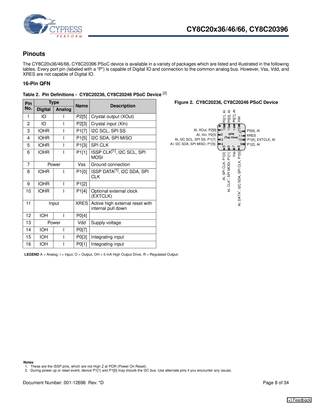
The CY8C20x36/46/66, CY8C20396 PSoC device is available in a variety of packages which are listed and illustrated in the following tables. Every port pin (labeled with a “P”) is capable of Digital IO and connection to the common analog bus. However, Vss, Vdd, and XRES are not capable of Digital IO.
16-Pin QFN
Table 2. Pin Definitions - CY8C20236, CY8C20246 PSoC Device [2] |
|
|
|
|
|
|
|
|
|
|
|
| |||||
|
|
|
|
|
| Figure 2. CY8C20236, CY8C20246 PSoC Device | |||||||||||
Pin | Type | Name | Description |
| |||||||||||||
No. | Digital | Analog |
|
|
| AI | AI | AI |
|
|
|
| |||||
1 | IO | I | P2[5] | Crystal output (XOut) |
|
|
| P0[1], | P0[3], | P0[7], | Vdd |
|
| ||||
|
|
|
|
|
|
|
|
|
|
|
|
| |||||
|
|
|
|
|
|
|
|
|
|
|
|
|
|
|
|
|
|
2 | IO | I | P2[3] | Crystal input (XIn) |
|
|
|
|
|
|
|
|
|
|
|
|
|
|
|
|
|
|
|
|
|
|
|
|
|
| |||||
|
|
|
|
|
| AI, XOut, P2[5] |
| 16 | 15 | 14 13 |
|
| |||||
3 | IOHR | I | P1[7] | I2C SCL, SPI SS |
|
|
| ||||||||||
| 1 |
|
|
|
| P0[4], AI | |||||||||||
| AI, XIn, P2[3] |
| 2 |
|
| QFN | 12 |
| |||||||||
|
|
|
|
|
|
|
|
| 11 |
| XRES | ||||||
4 | IOHR | I | P1[5] | I2C SDA, SPI MISO |
| AI, I2C SCL, SPI SS, P1[7] |
| 3 (Top View)10 |
| P1[4], EXTCLK, AI | |||||||
|
|
| |||||||||||||||
5 | IOHR | I | P1[3] | SPI CLK |
| AI, I2C SDA, SPI MISO, P1[5] |
| 4 |
|
|
|
|
| 9 |
| P1[2], AI | |
|
| 5 6 7 8 |
|
| |||||||||||||
6 | IOHR | I | P1[1] | ISSP CLK[1], I2C SCL, SPI |
|
|
|
|
|
|
|
|
|
|
|
|
|
|
|
| P1[3]CLK,SPIAI, | CLK | Vss | P1[0]CLK,SPISDA,I2C |
|
| |||||||||
|
|
|
| MOSI |
|
|
|
|
| ||||||||
|
|
|
|
|
|
|
|
| P1[1] |
|
|
|
|
|
| ||
|
|
|
|
|
|
|
|
|
| MOSI, |
|
|
|
|
|
| |
7 | Power | Vss | Ground connection |
|
|
|
|
|
|
|
|
|
|
| |||
|
|
|
|
|
|
|
|
|
|
|
|
| |||||
|
|
|
|
|
|
|
|
|
|
|
|
|
|
|
|
|
|
8 | IOHR | I | P1[0] | ISSP DATA[1], I2C SDA, SPI |
|
|
|
|
| , SPI |
|
|
|
|
|
| |
|
|
|
| CLK |
|
|
|
|
|
|
|
|
|
|
| ||
|
|
|
|
|
|
|
|
|
| 1 |
|
|
|
|
|
|
|
9 | IOHR | I | P1[2] |
|
|
|
|
|
| AI, |
|
|
|
|
|
| |
|
|
|
|
|
|
|
|
|
|
|
|
|
|
|
| ||
10 | IOHR | I | P1[4] | Optional external clock |
|
|
|
|
|
|
| 1 |
|
|
| ||
|
|
|
|
|
|
|
|
|
|
|
|
|
| , |
|
| |
|
|
|
| (EXTCLK) |
|
|
|
|
|
|
|
|
| DATA |
|
| |
|
|
|
|
|
|
|
|
|
|
|
|
|
|
|
| ||
11 | Input | XRES | Active high external reset with |
|
|
|
|
|
|
|
|
| AI, |
|
| ||
|
|
|
| internal pull down |
|
|
|
|
|
|
|
|
|
|
|
|
|
12 | IOH | I | P0[4] |
|
|
|
|
|
|
|
|
|
|
|
|
|
|
|
|
|
|
|
|
|
|
|
|
|
|
|
|
|
|
|
|
13 | Power | Vdd | Supply voltage |
|
|
|
|
|
|
|
|
|
|
|
|
| |
|
|
|
|
|
|
|
|
|
|
|
|
|
|
|
|
|
|
14 | IOH | I | P0[7] |
|
|
|
|
|
|
|
|
|
|
|
|
|
|
|
|
|
|
|
|
|
|
|
|
|
|
|
|
|
|
|
|
15 | IOH | I | P0[3] | Integrating input |
|
|
|
|
|
|
|
|
|
|
|
|
|
|
|
|
|
|
|
|
|
|
|
|
|
|
|
|
|
|
|
16 | IOH | I | P0[1] | Integrating input |
|
|
|
|
|
|
|
|
|
|
|
|
|
|
|
|
|
|
|
|
|
|
|
|
|
|
|
|
|
|
|
LEGEND A = Analog, I = Input, O = Output, OH = 5 mA High Output Drive, R = Regulated Output.
Notes
1.These are the ISSP pins, which are not High Z at POR (Power On Reset).
2.During power up or reset event, device P1[1] and P1[0] may disturb the I2C bus. Use alternate pins if you encounter any issues.
Document Number: | Page 8 of 34 |
[+] Feedback