CY8C20x36/46/66, CY8C20396
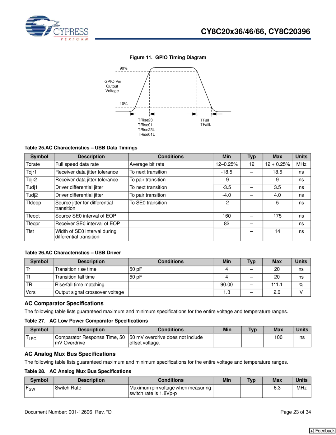
Figure 11. GPIO Timing Diagram
90% |
|
GPIO Pin |
|
Output |
|
Voltage |
|
10% |
|
TRise23 | TFall |
TRise01 | TFallL |
TRise23L
TRise01L
Table 25.AC Characteristics – USB Data Timings
Symbol | Description | Conditions | Min | Typ | Max | Units |
Tdrate | Full speed data rate | Average bit rate | 12 | 12 + 0.25% | MHz | |
|
|
|
|
|
|
|
Tdjr1 | Receiver data jitter tolerance | To next transition | – | 18.5 | ns | |
|
|
|
|
|
|
|
Tdjr2 | Receiver data jitter tolerance | To pair transition | – | 9 | ns | |
|
|
|
|
|
|
|
Tudj1 | Driver differential jitter | To next transition | – | 3.5 | ns | |
|
|
|
|
|
|
|
Tudj2 | Driver differential jitter | To pair transition | – | 4.0 | ns | |
|
|
|
|
|
|
|
Tfdeop | Source jitter for differential | To SE0 transition | – | 5 | ns | |
| transition |
|
|
|
|
|
Tfeopt | Source SE0 interval of EOP |
| 160 | – | 175 | ns |
|
|
|
|
|
|
|
Tfeopr | Receiver SE0 interval of EOP |
| 82 | – |
| ns |
|
|
|
|
|
|
|
Tfst | Width of SE0 interval during |
|
| – | 14 | ns |
| differential transition |
|
|
|
|
|
Table 26.AC Characteristics – USB Driver |
|
|
|
|
| |
|
|
|
|
|
|
|
Symbol | Description | Conditions | Min | Typ | Max | Units |
Tr | Transition rise time | 50 pF | 4 | – | 20 | ns |
|
|
|
|
|
|
|
Tf | Transition fall time | 50 pF | 4 | – | 20 | ns |
|
|
|
|
|
|
|
TR | Rise/fall time matching |
| 90.00 | – | 111.1 | % |
|
|
|
|
|
|
|
Vcrs | Output signal crossover voltage |
| 1.3 | – | 2.0 | V |
|
|
|
|
|
|
|
AC Comparator Specifications
The following table lists guaranteed maximum and minimum specifications for the entire voltage and temperature ranges.
Table 27. AC Low Power Comparator Specifications
Symbol | Description | Conditions | Min | Typ | Max | Units |
TLPC | Comparator Response Time, 50 | 50 mV overdrive does not include |
|
| 100 | ns |
| mV Overdrive | offset voltage. |
|
|
|
|
AC Analog Mux Bus Specifications
The following table lists guaranteed maximum and minimum specifications for the entire voltage and temperature ranges.
Table 28. AC Analog Mux Bus Specifications
Symbol | Description | Conditions | Min | Typ | Max | Units |
FSW | Switch Rate | Maximum pin voltage when measuring | – | – | 6.3 | MHz |
|
| switch rate is |
|
|
|
|
Document Number: |
|
|
| Page 23 of 34 | ||
[+] Feedback